DK-DEV-1AGX60N Altera, DK-DEV-1AGX60N Datasheet - Page 152
DK-DEV-1AGX60N
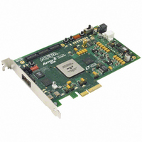
Manufacturer Part Number
DK-DEV-1AGX60N
Description
KIT DEV ARRIA GX 1AGX60N
Manufacturer
Altera
Series
Arria GXr
Type
FPGAr
Datasheet
1.EP1AGX20CF484C6N.pdf
(234 pages)
Specifications of DK-DEV-1AGX60N
Contents
Dev. Board, Quartus® II Web Edition, Reference Designs, Labs, and Complete Documentation
For Use With/related Products
1AGX60N
Lead Free Status / RoHS Status
Lead free / RoHS Compliant
Other names
544-2372
Available stocks
Company
Part Number
Manufacturer
Quantity
Price


4–30
Table 4–45. Timing Measurement Methodology for Input Pins
Arria GX Device Handbook, Volume 1
LVTTL
LVCMOS
2.5 V
1.8 V
1.5 V
PCI
PCI-X
SSTL-2 Class I
SSTL-2 Class II
SSTL-18 Class I
SSTL-18 Class II
1.8-V HSTL Class I
1.8-V HSTL Class II
1.5-V HSTL Class I
1.5-V HSTL Class II
1.2-V HSTL with OCT
Differential SSTL-2 Class I
Differential SSTL-2 Class II
Differential SSTL-18 Class I
(6)
(5)
(5)
(5)
(6)
(5)
(5)
I/O Standard
Figure 4–9. Measurement Setup for t
Table 4–45
Din
Din
OE
OE
specifies the input timing measurement setup.
V
3.135
3.135
2.375
1.710
1.425
2.970
2.970
2.325
2.325
1.660
1.660
1.660
1.660
1.375
1.375
1.140
2.325
2.325
1.660
CCIO
(V)
Measurement Conditions
zx
t
t
1 MΩ
1 MΩ
ZX
V
ZX
1.163
1.163
0.830
0.830
0.830
0.830
0.688
0.688
0.570
1.163
1.163
0.830
REF
, Tristate to Driving High
Dout
Dout
, Tristate to Driving Low
(Note
—
—
—
—
—
—
—
(V)
Dout
Dout
1), (2), (3),
Din
Din
OE
OE
Disable
Disable
Edge Rate (ns)
3.135
3.135
2.375
1.710
1.425
2.970
2.970
2.325
2.325
1.660
1.660
1.660
1.660
1.375
1.375
1.140
2.325
2.325
1.660
(4)
Chapter 4: DC and Switching Characteristics
Enable
Enable
(Part 1 of 2)
½ V
½ V
© December 2009 Altera Corporation
CCINT
CCINT
t
t
zh
zl
Measurement Point
VMEAS (V)
1.5675
1.5675
1.1875
0.7125
1.1625
1.1625
0.6875
0.6875
1.1625
1.1625
0.855
1.485
1.485
0.570
0.83
0.83
0.83
0.83
0.83
½ V
½ V
“1”
“0”
CCIO
CCIO
I/O Timing Model
Related parts for DK-DEV-1AGX60N
Image
Part Number
Description
Manufacturer
Datasheet
Request
R

Part Number:
Description:
KIT DEV ARRIA II GX FPGA 2AGX125
Manufacturer:
Altera
Datasheet:

Part Number:
Description:
KIT DEV CYCLONE III LS EP3CLS200
Manufacturer:
Altera
Datasheet:

Part Number:
Description:
KIT DEV STRATIX IV FPGA 4SE530
Manufacturer:
Altera
Datasheet:

Part Number:
Description:
KIT DEV FPGA 2AGX260 W/6.375G TX
Manufacturer:
Altera
Datasheet:

Part Number:
Description:
KIT DEV MAX V 5M570Z
Manufacturer:
Altera
Datasheet:

Part Number:
Description:
KIT DEV STRATIX V FPGA 5SGXEA7
Manufacturer:
Altera
Datasheet:

Part Number:
Description:
KIT DEVELOPMENT STRATIX III
Manufacturer:
Altera
Datasheet:

Part Number:
Description:
KIT DEVELOPMENT STRATIX IV
Manufacturer:
Altera
Datasheet:
Part Number:
Description:
KIT STARTER CYCLONE IV GX
Manufacturer:
Altera
Datasheet:
Part Number:
Description:
KIT DEVELOPMENT STRATIX IV
Manufacturer:
Altera
Datasheet:

Part Number:
Description:
CPLD, EP610 Family, ECMOS Process, 300 Gates, 16 Macro Cells, 16 Reg., 16 User I/Os, 5V Supply, 35 Speed Grade, 24DIP
Manufacturer:
Altera Corporation
Datasheet:
Part Number:
Description:
CPLD, EP610 Family, ECMOS Process, 300 Gates, 16 Macro Cells, 16 Reg., 16 User I/Os, 5V Supply, 15 Speed Grade, 24DIP
Manufacturer:
Altera Corporation
Datasheet: