DK-DEV-1AGX60N Altera, DK-DEV-1AGX60N Datasheet - Page 117
DK-DEV-1AGX60N
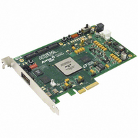
Manufacturer Part Number
DK-DEV-1AGX60N
Description
KIT DEV ARRIA GX 1AGX60N
Manufacturer
Altera
Series
Arria GXr
Type
FPGAr
Datasheet
1.EP1AGX20CF484C6N.pdf
(234 pages)
Specifications of DK-DEV-1AGX60N
Contents
Dev. Board, Quartus® II Web Edition, Reference Designs, Labs, and Complete Documentation
For Use With/related Products
1AGX60N
Lead Free Status / RoHS Status
Lead free / RoHS Compliant
Other names
544-2372
Available stocks
Company
Part Number
Manufacturer
Quantity
Price


Chapter 3: Configuration and Testing
Configuration
Configuration Schemes
Table 3–4. Arria GX Configuration Features (Part 1 of 2)
© December 2009 Altera Corporation
FPP
AS
PS
PPA
Configuration Scheme
f
f
V
on-the-fly or during a reconfiguration. The V
and must be hard-wired to V
1.8-V/1.5-V input buffer, and a logic low selects the 3.3-V/2.5-V input buffer. V
should be set to comply with the logic levels driven out of the configuration device or
MAX II microprocessor.
If the design must support configuration input voltages of 3.3 V/2.5 V, set V
logic low. You can set the V
inputs to any supported voltage. If the design must support configuration input
voltages of 1.8 V/1.5 V, set V
contains the configuration inputs to 1.8 V/1.5 V.
For more information about multi-volt support, including information about using
TDO and nCEO in multi-volt systems, refer to the
You can load the configuration data for an Arria GX device with one of five
configuration schemes (refer to
application. You can use a configuration device, intelligent controller, or the JTAG
port to configure an Arria GX device. A configuration device can automatically
configure an Arria GX device at system power up.
You can configure multiple Arria GX devices in any of the five configuration schemes
by connecting the configuration enable (nCE) and configuration enable output (nCEO)
pins on each device. Arria GX FPGAs offer the following:
■
■
Table 3–4
For more information about configuration schemes in Arria GX devices, refer to the
Configuring Arria GX Devices
CCSEL
Configuration data decompression to reduce configuration file storage
Remote system upgrades for remotely updating Arria GX designs
MAX II device or microprocessor
and flash device
Enhanced configuration device
Serial configuration device
MAX II device or microprocessor
and flash device
Enhanced configuration device
Download cable
MAX II device or microprocessor
and flash device
is sampled during power up. Therefore, the V
Configuration Method
lists which configuration features can be used in each configuration scheme.
(4)
CCIO
C CPD
CCSEL
chapter.
voltage of the I/O bank that contains the configuration
Table
or ground. A logic high V
to a logic high and the V
3–4), chosen on the basis of the target
Decompression
CCSEL
v
v
v
v
v
v
—
(1)
(2)
Arria GX Architecture
input buffer is powered by V
CCSEL
setting cannot change
CC SEL
Arria GX Device Handbook, Volume 1
CCIO
Remote System Upgrade
connection selects the
of the bank that
v
chapter.
v
v
v
v
—
v
(3)
CCSEL
CCINT
CCSEL
to a
3–5
Related parts for DK-DEV-1AGX60N
Image
Part Number
Description
Manufacturer
Datasheet
Request
R

Part Number:
Description:
KIT DEV ARRIA II GX FPGA 2AGX125
Manufacturer:
Altera
Datasheet:

Part Number:
Description:
KIT DEV CYCLONE III LS EP3CLS200
Manufacturer:
Altera
Datasheet:

Part Number:
Description:
KIT DEV STRATIX IV FPGA 4SE530
Manufacturer:
Altera
Datasheet:

Part Number:
Description:
KIT DEV FPGA 2AGX260 W/6.375G TX
Manufacturer:
Altera
Datasheet:

Part Number:
Description:
KIT DEV MAX V 5M570Z
Manufacturer:
Altera
Datasheet:

Part Number:
Description:
KIT DEV STRATIX V FPGA 5SGXEA7
Manufacturer:
Altera
Datasheet:

Part Number:
Description:
KIT DEVELOPMENT STRATIX III
Manufacturer:
Altera
Datasheet:

Part Number:
Description:
KIT DEVELOPMENT STRATIX IV
Manufacturer:
Altera
Datasheet:
Part Number:
Description:
KIT STARTER CYCLONE IV GX
Manufacturer:
Altera
Datasheet:
Part Number:
Description:
KIT DEVELOPMENT STRATIX IV
Manufacturer:
Altera
Datasheet:

Part Number:
Description:
CPLD, EP610 Family, ECMOS Process, 300 Gates, 16 Macro Cells, 16 Reg., 16 User I/Os, 5V Supply, 35 Speed Grade, 24DIP
Manufacturer:
Altera Corporation
Datasheet:
Part Number:
Description:
CPLD, EP610 Family, ECMOS Process, 300 Gates, 16 Macro Cells, 16 Reg., 16 User I/Os, 5V Supply, 15 Speed Grade, 24DIP
Manufacturer:
Altera Corporation
Datasheet: