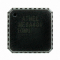
ATMEGA48V-10MU Atmel, ATMEGA48V-10MU Datasheet - Page 228

ATMEGA48V-10MU
Manufacturer Part Number
ATMEGA48V-10MU
Description
IC AVR MCU 4K 10MHZ 1.8V 32-QFN
Manufacturer
Atmel
Series
AVR® ATmegar
Specifications of ATMEGA48V-10MU
Core Processor
AVR
Core Size
8-Bit
Speed
10MHz
Connectivity
I²C, SPI, UART/USART
Peripherals
Brown-out Detect/Reset, POR, PWM, WDT
Number Of I /o
23
Program Memory Size
4KB (2K x 16)
Program Memory Type
FLASH
Eeprom Size
256 x 8
Ram Size
512 x 8
Voltage - Supply (vcc/vdd)
1.8 V ~ 5.5 V
Data Converters
A/D 8x10b
Oscillator Type
Internal
Operating Temperature
-40°C ~ 85°C
Package / Case
32-VQFN Exposed Pad, 32-HVQFN, 32-SQFN, 32-DHVQFN
Package
32MLF EP
Device Core
AVR
Family Name
ATmega
Maximum Speed
10 MHz
Operating Supply Voltage
2.5|3.3|5 V
Data Bus Width
8 Bit
Number Of Programmable I/os
23
Interface Type
SPI/TWI/USART
On-chip Adc
8-chx10-bit
Number Of Timers
3
Processor Series
ATMEGA48x
Core
AVR8
Data Ram Size
512 B
Maximum Clock Frequency
10 MHz
Maximum Operating Temperature
+ 85 C
Mounting Style
SMD/SMT
3rd Party Development Tools
EWAVR, EWAVR-BL
Minimum Operating Temperature
- 40 C
Controller Family/series
AVR MEGA
No. Of I/o's
23
Eeprom Memory Size
256Byte
Ram Memory Size
512Byte
Cpu Speed
10MHz
No. Of Timers
3
Rohs Compliant
Yes
For Use With
ATSTK600-TQFP32 - STK600 SOCKET/ADAPTER 32-TQFPATSTK600-DIP40 - STK600 SOCKET/ADAPTER 40-PDIP770-1007 - ISP 4PORT ATMEL AVR MCU SPI/JTAGATAVRDRAGON - KIT DRAGON 32KB FLASH MEM AVRATAVRISP2 - PROGRAMMER AVR IN SYSTEMATJTAGICE2 - AVR ON-CHIP D-BUG SYSTEM
Lead Free Status / RoHS Status
Lead free / RoHS Compliant
Available stocks
Company
Part Number
Manufacturer
Quantity
Price
- Current page: 228 of 378
- Download datasheet (8Mb)
228
ATmega48/88/168
The upper 7 bits are the address to which the 2-wire Serial Interface will respond when
addressed by a Master. If the LSB is set, the TWI will respond to the general call address (0x00),
otherwise it will ignore the general call address.
TWEN must be written to one to enable the TWI. The TWEA bit must be written to one to enable
the acknowledgement of the device’s own slave address or the general call address. TWSTA
and TWSTO must be written to zero.
When TWAR and TWCR have been initialized, the TWI waits until it is addressed by its own
slave address (or the general call address if enabled) followed by the data direction bit. If the
direction bit is “0” (write), the TWI will operate in SR mode, otherwise ST mode is entered. After
its own slave address and the write bit have been received, the TWINT Flag is set and a valid
status code can be read from TWSR. The status code is used to determine the appropriate soft-
ware action. The appropriate action to be taken for each status code is detailed in
The Slave Receiver mode may also be entered if arbitration is lost while the TWI is in the Master
mode (see states 0x68 and 0x78).
If the TWEA bit is reset during a transfer, the TWI will return a “Not Acknowledge” (“1”) to SDA
after the next received data byte. This can be used to indicate that the Slave is not able to
receive any more bytes. While TWEA is zero, the TWI does not acknowledge its own slave
address. However, the 2-wire Serial Bus is still monitored and address recognition may resume
at any time by setting TWEA. This implies that the TWEA bit may be used to temporarily isolate
the TWI from the 2-wire Serial Bus.
In all sleep modes other than Idle mode, the clock system to the TWI is turned off. If the TWEA
bit is set, the interface can still acknowledge its own slave address or the general call address by
using the 2-wire Serial Bus clock as a clock source. The part will then wake up from sleep and
the TWI will hold the SCL clock low during the wake up and until the TWINT Flag is cleared (by
writing it to one). Further data reception will be carried out as normal, with the AVR clocks run-
ning as normal. Observe that if the AVR is set up with a long start-up time, the SCL line may be
held low for a long time, blocking other data transmissions.
Note that the 2-wire Serial Interface Data Register – TWDR does not reflect the last byte present
on the bus when waking up from these Sleep modes.
TWCR
value
TWINT
0
TWEA
1
TWSTA
0
TWSTO
0
TWWC
0
TWEN
1
–
0
2545S–AVR–07/10
Table
TWIE
X
21-4.
Related parts for ATMEGA48V-10MU
Image
Part Number
Description
Manufacturer
Datasheet
Request
R

Part Number:
Description:
IC AVR MCU 4K 5V 10MHZ 32-TQFP
Manufacturer:
Atmel
Datasheet:

Part Number:
Description:
IC AVR MCU 4K 10MHZ 1.8V 28DIP
Manufacturer:
Atmel
Datasheet:

Part Number:
Description:
MCU AVR 4K FLASH 10MHZ 28-QFN
Manufacturer:
Atmel
Datasheet:

Part Number:
Description:
IC AVR MCU 4K 5V 10MHZ 32-TQFP
Manufacturer:
Atmel
Datasheet:

Part Number:
Description:
IC AVR MCU 4K 5V 12MHZ 32-QFN
Manufacturer:
Atmel
Datasheet:

Part Number:
Description:
IC AVR MCU 4K 5V 10MHZ 32-QFN
Manufacturer:
Atmel
Datasheet:

Part Number:
Description:
IC AVR MCU 4K 5V 10MHZ 28-DIP
Manufacturer:
Atmel
Datasheet:

Part Number:
Description:
IC AVR MCU 4K 5V 10MHZ 28-DIP
Manufacturer:
Atmel
Datasheet:

Part Number:
Description:
MCU AVR 4KB FLASH 10MHZ 32TQFP
Manufacturer:
Atmel
Datasheet:

Part Number:
Description:
MCU AVR 4KB FLASH 10MHZ 32QFN
Manufacturer:
Atmel
Datasheet:

Part Number:
Description:
MCU AVR 4KB FLASH 20MHZ 28QFN
Manufacturer:
Atmel
Datasheet:


