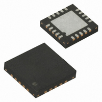
ATTINY84V-10MU Atmel, ATTINY84V-10MU Datasheet - Page 108

ATTINY84V-10MU
Manufacturer Part Number
ATTINY84V-10MU
Description
IC MCU AVR 8K FLASH 10MHZ 20-QFN
Manufacturer
Atmel
Series
AVR® ATtinyr
Specifications of ATTINY84V-10MU
Core Processor
AVR
Core Size
8-Bit
Speed
10MHz
Connectivity
USI
Peripherals
Brown-out Detect/Reset, POR, PWM, Temp Sensor, WDT
Number Of I /o
12
Program Memory Size
8KB (4K x 16)
Program Memory Type
FLASH
Eeprom Size
512 x 8
Ram Size
512 x 8
Voltage - Supply (vcc/vdd)
1.8 V ~ 5.5 V
Data Converters
A/D 8x10b
Oscillator Type
Internal
Operating Temperature
-40°C ~ 85°C
Package / Case
20-MLF®, QFN
Processor Series
ATTINY8x
Core
AVR8
Data Bus Width
8 bit
Data Ram Size
512 B
Interface Type
SPI
Maximum Clock Frequency
10 MHz
Number Of Programmable I/os
12
Number Of Timers
2
Maximum Operating Temperature
+ 85 C
Mounting Style
SMD/SMT
Minimum Operating Temperature
- 40 C
On-chip Adc
8-ch x 10-bit
For Use With
ATSTK600 - DEV KIT FOR AVR/AVR32770-1007 - ISP 4PORT ATMEL AVR MCU SPI/JTAGATAVRISP2 - PROGRAMMER AVR IN SYSTEM
Lead Free Status / RoHS Status
Lead free / RoHS Compliant
- Current page: 108 of 238
- Download datasheet (5Mb)
12.10.1
12.11 Register Description
12.11.1
108
ATtiny24/44/84
Reusing the Temporary High Byte Register
TCCR1A – Timer/Counter1 Control Register A
Note:
The assembly code example requires that the r17:r16 register pair contains the value to be writ-
ten to TCNT1.
If writing to more than one 16-bit register where the high byte is the same for all registers written,
then the high byte only needs to be written once. However, note that the same rule of atomic
operation described previously also applies in this case.
• Bits 7:6 – COM1A1, COM1A0: Compare Output Mode for Channel A
• Bits 5:4 – COM1B1, COM1B0: Compare Output Mode for Channel B
The COM1A1:0 and COM1B1:0 control the Output Compare pins (OC1A and OC1B respec-
tively) behavior. If one or both of the COM1A1:0 bits are written to one, the OC1A output
overrides the normal port functionality of the I/O pin it is connected to. If one or both of the
COM1B1:0 bit are written to one, the OC1B output overrides the normal port functionality of the
I/O pin it is connected to. However, note that the Data Direction Register (DDR) bit correspond-
ing to the OC1A or OC1B pin must be set in order to enable the output driver.
When the OC1A or OC1B is connected to the pin, the function of the COM1x1:0 bits is depen-
dent of the WGM13:0 bits setting.
when the WGM13:0 bits are set to a Normal or a CTC mode (non-PWM).
Bit
0x2F (0x4F)
Read/Write
Initial Value
C Code Example
void TIM16_WriteTCNT1( unsigned int i )
{
}
unsigned char sreg;
unsigned int i;
/* Save global interrupt flag */
sreg = SREG;
/* Disable interrupts */
_CLI();
/* Set TCNT1 to i */
TCNT1 = i;
/* Restore global interrupt flag */
SREG = sreg;
See
“Code Examples” on page
COM1A1
R/W
7
0
COM1A0
R/W
6
0
COM1B1
Table 12-2 on page 109
R/W
5
0
6.
COM1B0
R/W
4
0
R
3
–
0
shows the COM1x1:0 bit functionality
R
2
–
0
WGM11
R/W
1
0
WGM10
R/W
0
0
8006K–AVR–10/10
TCCR1A
Related parts for ATTINY84V-10MU
Image
Part Number
Description
Manufacturer
Datasheet
Request
R

Part Number:
Description:
MCU AVR 8KB FLASH 10MHZ 14SOIC
Manufacturer:
Atmel
Datasheet:

Part Number:
Description:
MCU AVR 8KB FLASH 10MHZ 20QFN
Manufacturer:
Atmel
Datasheet:

Part Number:
Description:
MCU AVR 8K ISP FLASH 1.8V 14SOIC
Manufacturer:
Atmel
Datasheet:

Part Number:
Description:
AVR MCU, 8K FLASH, 512B RAM, 512B EE
Manufacturer:
Atmel
Datasheet:

Part Number:
Description:
Manufacturer:
Atmel Corporation
Datasheet:

Part Number:
Description:
Manufacturer:
Atmel Corporation
Datasheet:

Part Number:
Description:
IC MCU AVR 8K FLASH 20MHZ 20-QFN
Manufacturer:
Atmel
Datasheet:

Part Number:
Description:
MCU AVR 8K ISP FLASH 2.7V 14SOIC
Manufacturer:
Atmel
Datasheet:

Part Number:
Description:
MCU AVR 8K FLASH 15MHZ 20-QFN
Manufacturer:
Atmel
Datasheet:

Part Number:
Description:
IC MCU AVR 8K FLASH 20MHZ 14-DIP
Manufacturer:
Atmel
Datasheet:

Part Number:
Description:
MCU AVR 8KB FLASH 10MHZ 14SOIC
Manufacturer:
Atmel
Datasheet:

Part Number:
Description:
MCU AVR 8KB FLASH 20MHZ 20QFN
Manufacturer:
Atmel
Datasheet:

Part Number:
Description:
IC, MCU, 8BIT, 2K FLASH, 20SOIC
Manufacturer:
Atmel
Datasheet:

Part Number:
Description:
IC, MCU, 8BIT, 2K FLASH, 20PDIP
Manufacturer:
Atmel
Datasheet:

Part Number:
Description:
IC, MCU, 8BIT, 8K FLASH, 20PDIP
Manufacturer:
Atmel
Datasheet:


