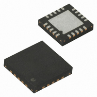
ATTINY84V-10MU Atmel, ATTINY84V-10MU Datasheet - Page 171

ATTINY84V-10MU
Manufacturer Part Number
ATTINY84V-10MU
Description
IC MCU AVR 8K FLASH 10MHZ 20-QFN
Manufacturer
Atmel
Series
AVR® ATtinyr
Specifications of ATTINY84V-10MU
Core Processor
AVR
Core Size
8-Bit
Speed
10MHz
Connectivity
USI
Peripherals
Brown-out Detect/Reset, POR, PWM, Temp Sensor, WDT
Number Of I /o
12
Program Memory Size
8KB (4K x 16)
Program Memory Type
FLASH
Eeprom Size
512 x 8
Ram Size
512 x 8
Voltage - Supply (vcc/vdd)
1.8 V ~ 5.5 V
Data Converters
A/D 8x10b
Oscillator Type
Internal
Operating Temperature
-40°C ~ 85°C
Package / Case
20-MLF®, QFN
Processor Series
ATTINY8x
Core
AVR8
Data Bus Width
8 bit
Data Ram Size
512 B
Interface Type
SPI
Maximum Clock Frequency
10 MHz
Number Of Programmable I/os
12
Number Of Timers
2
Maximum Operating Temperature
+ 85 C
Mounting Style
SMD/SMT
Minimum Operating Temperature
- 40 C
On-chip Adc
8-ch x 10-bit
For Use With
ATSTK600 - DEV KIT FOR AVR/AVR32770-1007 - ISP 4PORT ATMEL AVR MCU SPI/JTAGATAVRISP2 - PROGRAMMER AVR IN SYSTEM
Lead Free Status / RoHS Status
Lead free / RoHS Compliant
- Current page: 171 of 238
- Download datasheet (5Mb)
19.7.6
19.7.7
19.7.8
19.7.9
19.7.10
Table 19-16. High-voltage Serial Programming Instruction Set for ATtiny24/44/84
8006K–AVR–10/10
Instruction
Chip Erase
Load “Write
Flash”
Command
Load Flash
Page Buffer
Load Flash
High Address
and Program
Page
Reading the Flash
Reading the EEPROM
Programming and Reading the Fuse and Lock Bits
Reading the Signature Bytes and Calibration Byte
Power-off sequence
SDI
SII
SDO
SDI
SII
SDO
SDI
SII
SDO
SDI
SII
SDO
SDI
SII
SDO
0_1000_0000_00
0_0100_1100_00
x_xxxx_xxxx_xx
0_0001_0000_00
0_0100_1100_00
x_xxxx_xxxx_xx
0_ bbbb_bbbb _00
0_0000_1100_00
x_xxxx_xxxx_xx
0_dddd_dddd_00
0_0011_1100_00
x_xxxx_xxxx_xx
0_0000_000a_00
0_0001_1100_00
x_xxxx_xxxx_xx
The algorithm for reading the Flash memory is as follows (refer to
The algorithm for reading the EEPROM memory is as follows (refer to
171):
The algorithms for programming and reading the Fuse Low/High bits and Lock bits are shown in
Table 19-16 on page
The algorithms for reading the Signature bytes and Calibration byte are shown in
page
Set SCI to “0”. Set RESET to “1”. Turn V
Instr.1/5
1. Load Command "Read Flash".
2. Read Flash Low and High Bytes. The contents at the selected address are available at
1. Load Command “Read EEPROM”.
2. Read EEPROM Byte. The contents at the selected address are available at serial out-
serial output SDO.
put SDO.
171.
0_0000_0000_00
0_0110_0100_00
x_xxxx_xxxx_xx
0_eeee_eeee_00
0_0010_1100_00
x_xxxx_xxxx_xx
0_0000_0000_00
0_0111_1101_00
x_xxxx_xxxx_xx
0_0000_0000_00
0_0110_0100_00
x_xxxx_xxxx_xx
Instr.2/6
171.
Instruction Format
0_0000_0000_00
0_0110_1100_00
x_xxxx_xxxx_xx
0_0000_0000_00
0_0110_1101_00
x_xxxx_xxxx_xx
0_0000_0000_00
0_0111_1100_00
x_xxxx_xxxx_xx
0_0000_0000_00
0_0110_1100_00
x_xxxx_xxxx_xx
Instr.3/7
CC
power off.
0_0000_0000_00
0_0110_1100_00
x_xxxx_xxxx_xx
Instr.4
Table 19-16 on page
ATtiny24/44/84
Operation Remarks
Wait after Instr.3 until SDO
goes high for the Chip Erase
cycle to finish.
Enter Flash Programming code.
Repeat after Instr. 1 - 7until the
entire page buffer is filled or
until all data within the page is
filled.
Wait after Instr 3 until SDO
goes high. Repeat Instr. 2 - 3
for each loaded Flash Page
until the entire Flash or all data
is programmed. Repeat Instr. 1
for a new 256 byte page.
Instr 5-7.
(2)
Table 19-16 on page
Table 19-16 on
171):
(2)
171
Related parts for ATTINY84V-10MU
Image
Part Number
Description
Manufacturer
Datasheet
Request
R

Part Number:
Description:
MCU AVR 8KB FLASH 10MHZ 14SOIC
Manufacturer:
Atmel
Datasheet:

Part Number:
Description:
MCU AVR 8KB FLASH 10MHZ 20QFN
Manufacturer:
Atmel
Datasheet:

Part Number:
Description:
MCU AVR 8K ISP FLASH 1.8V 14SOIC
Manufacturer:
Atmel
Datasheet:

Part Number:
Description:
AVR MCU, 8K FLASH, 512B RAM, 512B EE
Manufacturer:
Atmel
Datasheet:

Part Number:
Description:
Manufacturer:
Atmel Corporation
Datasheet:

Part Number:
Description:
Manufacturer:
Atmel Corporation
Datasheet:

Part Number:
Description:
IC MCU AVR 8K FLASH 20MHZ 20-QFN
Manufacturer:
Atmel
Datasheet:

Part Number:
Description:
MCU AVR 8K ISP FLASH 2.7V 14SOIC
Manufacturer:
Atmel
Datasheet:

Part Number:
Description:
MCU AVR 8K FLASH 15MHZ 20-QFN
Manufacturer:
Atmel
Datasheet:

Part Number:
Description:
IC MCU AVR 8K FLASH 20MHZ 14-DIP
Manufacturer:
Atmel
Datasheet:

Part Number:
Description:
MCU AVR 8KB FLASH 10MHZ 14SOIC
Manufacturer:
Atmel
Datasheet:

Part Number:
Description:
MCU AVR 8KB FLASH 20MHZ 20QFN
Manufacturer:
Atmel
Datasheet:

Part Number:
Description:
IC, MCU, 8BIT, 2K FLASH, 20SOIC
Manufacturer:
Atmel
Datasheet:

Part Number:
Description:
IC, MCU, 8BIT, 2K FLASH, 20PDIP
Manufacturer:
Atmel
Datasheet:

Part Number:
Description:
IC, MCU, 8BIT, 8K FLASH, 20PDIP
Manufacturer:
Atmel
Datasheet:


