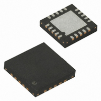
ATTINY84V-10MU Atmel, ATTINY84V-10MU Datasheet - Page 37

ATTINY84V-10MU
Manufacturer Part Number
ATTINY84V-10MU
Description
IC MCU AVR 8K FLASH 10MHZ 20-QFN
Manufacturer
Atmel
Series
AVR® ATtinyr
Specifications of ATTINY84V-10MU
Core Processor
AVR
Core Size
8-Bit
Speed
10MHz
Connectivity
USI
Peripherals
Brown-out Detect/Reset, POR, PWM, Temp Sensor, WDT
Number Of I /o
12
Program Memory Size
8KB (4K x 16)
Program Memory Type
FLASH
Eeprom Size
512 x 8
Ram Size
512 x 8
Voltage - Supply (vcc/vdd)
1.8 V ~ 5.5 V
Data Converters
A/D 8x10b
Oscillator Type
Internal
Operating Temperature
-40°C ~ 85°C
Package / Case
20-MLF®, QFN
Processor Series
ATTINY8x
Core
AVR8
Data Bus Width
8 bit
Data Ram Size
512 B
Interface Type
SPI
Maximum Clock Frequency
10 MHz
Number Of Programmable I/os
12
Number Of Timers
2
Maximum Operating Temperature
+ 85 C
Mounting Style
SMD/SMT
Minimum Operating Temperature
- 40 C
On-chip Adc
8-ch x 10-bit
For Use With
ATSTK600 - DEV KIT FOR AVR/AVR32770-1007 - ISP 4PORT ATMEL AVR MCU SPI/JTAGATAVRISP2 - PROGRAMMER AVR IN SYSTEM
Lead Free Status / RoHS Status
Lead free / RoHS Compliant
- Current page: 37 of 238
- Download datasheet (5Mb)
7.5.2
8006K–AVR–10/10
PRR – Power Reduction Register
both BODS and BODSE must be set to one. Second, within four clock cycles, BODS must be
set to one and BODSE must be set to zero. The BODS bit is active three clock cycles after it is
set. A sleep instruction must be executed while BODS is active in order to turn off the BOD for
the actual sleep mode. The BODS bit is automatically cleared after three clock cycles.
In devices where Sleeping BOD has not been implemented this bit is unused and will always
read zero.
• Bit 5 – SE: Sleep Enable
The SE bit must be written to logic one to make the MCU enter the sleep mode when the SLEEP
instruction is executed. To avoid the MCU entering the sleep mode unless it is the programmer’s
purpose, it is recommended to write the Sleep Enable (SE) bit to one just before the execution of
the SLEEP instruction and to clear it immediately after waking up.
• Bits 4:3 – SM1, SM0: Sleep Mode Select Bits 1:0
These bits select between the three available sleep modes as shown in
Table 7-2.
Note:
• Bit 2 – BODSE: BOD Sleep Enable
BOD disable functionality is available in some devices, only. See
The BODSE bit enables setting of BODS control bit, as explained on BODS bit description. BOD
disable is controlled by a timed sequence.
This bit is unused in devices where software BOD disable has not been implemented and will
read as zero in those devices.
The Power Reduction Register provides a method to reduce power consumption by allowing
peripheral clock signals to be disabled.
• Bits 7:4 – Res: Reserved Bits
These bits are reserved in the ATtiny24/44/84 and will always read as zero.
• Bit 3 – PRTIM1: Power Reduction Timer/Counter1
Writing a logic one to this bit shuts down the Timer/Counter1 module. When the Timer/Counter1
is enabled, operation will continue like before the shutdown.
Bit
Read/Write
Initial Value
SM1
1. Only recommended with external crystal or resonator selected as clock source
0
0
1
1
Sleep Mode Select
R
7
–
0
SM0
R
6
–
0
0
1
0
1
R
5
–
0
Sleep Mode
Idle
ADC Noise Reduction
Power-down
Standby
R
4
–
0
(1)
PRTIM1
R/W
3
0
PRTIM0
R/W
2
0
“Limitations” on page
ATtiny24/44/84
PRUSI
R/W
Table
1
0
7-2.
PRADC
R/W
0
0
35.
PRR
37
Related parts for ATTINY84V-10MU
Image
Part Number
Description
Manufacturer
Datasheet
Request
R

Part Number:
Description:
MCU AVR 8KB FLASH 10MHZ 14SOIC
Manufacturer:
Atmel
Datasheet:

Part Number:
Description:
MCU AVR 8KB FLASH 10MHZ 20QFN
Manufacturer:
Atmel
Datasheet:

Part Number:
Description:
MCU AVR 8K ISP FLASH 1.8V 14SOIC
Manufacturer:
Atmel
Datasheet:

Part Number:
Description:
AVR MCU, 8K FLASH, 512B RAM, 512B EE
Manufacturer:
Atmel
Datasheet:

Part Number:
Description:
Manufacturer:
Atmel Corporation
Datasheet:

Part Number:
Description:
Manufacturer:
Atmel Corporation
Datasheet:

Part Number:
Description:
IC MCU AVR 8K FLASH 20MHZ 20-QFN
Manufacturer:
Atmel
Datasheet:

Part Number:
Description:
MCU AVR 8K ISP FLASH 2.7V 14SOIC
Manufacturer:
Atmel
Datasheet:

Part Number:
Description:
MCU AVR 8K FLASH 15MHZ 20-QFN
Manufacturer:
Atmel
Datasheet:

Part Number:
Description:
IC MCU AVR 8K FLASH 20MHZ 14-DIP
Manufacturer:
Atmel
Datasheet:

Part Number:
Description:
MCU AVR 8KB FLASH 10MHZ 14SOIC
Manufacturer:
Atmel
Datasheet:

Part Number:
Description:
MCU AVR 8KB FLASH 20MHZ 20QFN
Manufacturer:
Atmel
Datasheet:

Part Number:
Description:
IC, MCU, 8BIT, 2K FLASH, 20SOIC
Manufacturer:
Atmel
Datasheet:

Part Number:
Description:
IC, MCU, 8BIT, 2K FLASH, 20PDIP
Manufacturer:
Atmel
Datasheet:

Part Number:
Description:
IC, MCU, 8BIT, 8K FLASH, 20PDIP
Manufacturer:
Atmel
Datasheet:


