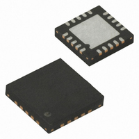
ATTINY84V-10MU Atmel, ATTINY84V-10MU Datasheet - Page 92

ATTINY84V-10MU
Manufacturer Part Number
ATTINY84V-10MU
Description
IC MCU AVR 8K FLASH 10MHZ 20-QFN
Manufacturer
Atmel
Series
AVR® ATtinyr
Specifications of ATTINY84V-10MU
Core Processor
AVR
Core Size
8-Bit
Speed
10MHz
Connectivity
USI
Peripherals
Brown-out Detect/Reset, POR, PWM, Temp Sensor, WDT
Number Of I /o
12
Program Memory Size
8KB (4K x 16)
Program Memory Type
FLASH
Eeprom Size
512 x 8
Ram Size
512 x 8
Voltage - Supply (vcc/vdd)
1.8 V ~ 5.5 V
Data Converters
A/D 8x10b
Oscillator Type
Internal
Operating Temperature
-40°C ~ 85°C
Package / Case
20-MLF®, QFN
Processor Series
ATTINY8x
Core
AVR8
Data Bus Width
8 bit
Data Ram Size
512 B
Interface Type
SPI
Maximum Clock Frequency
10 MHz
Number Of Programmable I/os
12
Number Of Timers
2
Maximum Operating Temperature
+ 85 C
Mounting Style
SMD/SMT
Minimum Operating Temperature
- 40 C
On-chip Adc
8-ch x 10-bit
For Use With
ATSTK600 - DEV KIT FOR AVR/AVR32770-1007 - ISP 4PORT ATMEL AVR MCU SPI/JTAGATAVRISP2 - PROGRAMMER AVR IN SYSTEM
Lead Free Status / RoHS Status
Lead free / RoHS Compliant
- Current page: 92 of 238
- Download datasheet (5Mb)
12.5.2
12.5.3
12.6
92
Output Compare Units
ATtiny24/44/84
Noise Canceler
Using the Input Capture Unit
Comparator Input Capture (ACIC) bit in the Analog Comparator Control and Status Register
(ACSR). Be aware that changing trigger source can trigger a capture. The Input Capture Flag
must therefore be cleared after the change.
Both the Input Capture pin (ICP1) and the Analog Comparator output (ACO) inputs are sampled
using the same technique as for the T1 pin
identical. However, when the noise canceler is enabled, additional logic is inserted before the
edge detector, which increases the delay by four system clock cycles. Note that the input of the
noise canceler and edge detector is always enabled unless the Timer/Counter is set in a Wave-
form Generation mode that uses ICR1 to define TOP.
An Input Capture can be triggered by software by controlling the port of the ICP1 pin.
The noise canceler uses a simple digital filtering technique to improve noise immunity. Consecu-
tive samples are monitored in a pipeline four units deep. The signal going to the edge detecter is
allowed to change only when all four samples are equal.
The noise canceler is enabled by setting the Input Capture Noise Canceler (ICNC1) bit in
Timer/Counter Control Register B (TCCR1B). When enabled, the noise canceler introduces an
additional delay of four system clock cycles to a change applied to the input and before ICR1 is
updated.
The noise canceler uses the system clock directly and is therefore not affected by the prescaler.
The main challenge when using the Input Capture unit is to assign enough processor capacity
for handling the incoming events. The time between two events is critical. If the processor has
not read the captured value in the ICR1 Register before the next event occurs, the ICR1 will be
overwritten with a new value. In this case the result of the capture will be incorrect.
When using the Input Capture interrupt, the ICR1 Register should be read as early in the inter-
rupt handler routine as possible. Even though the Input Capture interrupt has relatively high
priority, the maximum interrupt response time is dependent on the maximum number of clock
cycles it takes to handle any of the other interrupt requests.
Using the Input Capture unit in any mode of operation when the TOP value (resolution) is
actively changed during operation, is not recommended.
Measurement of an external signal’s duty cycle requires that the trigger edge is changed after
each capture. Changing the edge sensing must be done as early as possible after the ICR1
Register has been read. After a change of the edge, the Input Capture Flag (ICF1) must be
cleared by software (writing a logical one to the I/O bit location). For measuring frequency only,
the clearing of the ICF1 flag is not required (if an interrupt handler is used).
The 16-bit comparator continuously compares TCNT1 with the Output Compare Register
(OCR1x). If TCNT equals OCR1x the comparator signals a match. A match will set the Output
Compare Flag (OCF1x) at the next timer clock cycle. If enabled (OCIE1x = 1), the Output Com-
pare Flag generates an Output Compare interrupt. The OCF1x flag is automatically cleared
when the interrupt is executed. Alternatively the OCF1x flag can be cleared by software by writ-
ing a logical one to its I/O bit location. The Waveform Generator uses the match signal to
generate an output according to operating mode set by the Waveform Generation mode
(Figure 13-1 on page
115). The edge detector is also
8006K–AVR–10/10
Related parts for ATTINY84V-10MU
Image
Part Number
Description
Manufacturer
Datasheet
Request
R

Part Number:
Description:
MCU AVR 8KB FLASH 10MHZ 14SOIC
Manufacturer:
Atmel
Datasheet:

Part Number:
Description:
MCU AVR 8KB FLASH 10MHZ 20QFN
Manufacturer:
Atmel
Datasheet:

Part Number:
Description:
MCU AVR 8K ISP FLASH 1.8V 14SOIC
Manufacturer:
Atmel
Datasheet:

Part Number:
Description:
AVR MCU, 8K FLASH, 512B RAM, 512B EE
Manufacturer:
Atmel
Datasheet:

Part Number:
Description:
Manufacturer:
Atmel Corporation
Datasheet:

Part Number:
Description:
Manufacturer:
Atmel Corporation
Datasheet:

Part Number:
Description:
IC MCU AVR 8K FLASH 20MHZ 20-QFN
Manufacturer:
Atmel
Datasheet:

Part Number:
Description:
MCU AVR 8K ISP FLASH 2.7V 14SOIC
Manufacturer:
Atmel
Datasheet:

Part Number:
Description:
MCU AVR 8K FLASH 15MHZ 20-QFN
Manufacturer:
Atmel
Datasheet:

Part Number:
Description:
IC MCU AVR 8K FLASH 20MHZ 14-DIP
Manufacturer:
Atmel
Datasheet:

Part Number:
Description:
MCU AVR 8KB FLASH 10MHZ 14SOIC
Manufacturer:
Atmel
Datasheet:

Part Number:
Description:
MCU AVR 8KB FLASH 20MHZ 20QFN
Manufacturer:
Atmel
Datasheet:

Part Number:
Description:
IC, MCU, 8BIT, 2K FLASH, 20SOIC
Manufacturer:
Atmel
Datasheet:

Part Number:
Description:
IC, MCU, 8BIT, 2K FLASH, 20PDIP
Manufacturer:
Atmel
Datasheet:

Part Number:
Description:
IC, MCU, 8BIT, 8K FLASH, 20PDIP
Manufacturer:
Atmel
Datasheet:


