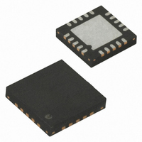
ATTINY84V-10MU Atmel, ATTINY84V-10MU Datasheet - Page 95

ATTINY84V-10MU
Manufacturer Part Number
ATTINY84V-10MU
Description
IC MCU AVR 8K FLASH 10MHZ 20-QFN
Manufacturer
Atmel
Series
AVR® ATtinyr
Specifications of ATTINY84V-10MU
Core Processor
AVR
Core Size
8-Bit
Speed
10MHz
Connectivity
USI
Peripherals
Brown-out Detect/Reset, POR, PWM, Temp Sensor, WDT
Number Of I /o
12
Program Memory Size
8KB (4K x 16)
Program Memory Type
FLASH
Eeprom Size
512 x 8
Ram Size
512 x 8
Voltage - Supply (vcc/vdd)
1.8 V ~ 5.5 V
Data Converters
A/D 8x10b
Oscillator Type
Internal
Operating Temperature
-40°C ~ 85°C
Package / Case
20-MLF®, QFN
Processor Series
ATTINY8x
Core
AVR8
Data Bus Width
8 bit
Data Ram Size
512 B
Interface Type
SPI
Maximum Clock Frequency
10 MHz
Number Of Programmable I/os
12
Number Of Timers
2
Maximum Operating Temperature
+ 85 C
Mounting Style
SMD/SMT
Minimum Operating Temperature
- 40 C
On-chip Adc
8-ch x 10-bit
For Use With
ATSTK600 - DEV KIT FOR AVR/AVR32770-1007 - ISP 4PORT ATMEL AVR MCU SPI/JTAGATAVRISP2 - PROGRAMMER AVR IN SYSTEM
Lead Free Status / RoHS Status
Lead free / RoHS Compliant
- Current page: 95 of 238
- Download datasheet (5Mb)
12.7.1
8006K–AVR–10/10
Compare Output Mode and Waveform Generation
Figure 12-5. Compare Match Output Unit, Schematic (non-PWM Mode)
The general I/O port function is overridden by the Output Compare (OC1x) from the Waveform
Generator if either of the COM1x1:0 bits are set. However, the OC1x pin direction (input or out-
put) is still controlled by the Data Direction Register (DDR) for the port pin. The Data Direction
Register bit for the OC1x pin (DDR_OC1x) must be set as output before the OC1x value is visi-
ble on the pin. The port override function is generally independent of the Waveform Generation
mode, but there are some exceptions. See
and
The design of the Output Compare pin logic allows initialization of the OC1x state before the out-
put is enabled. Note that some COM1x1:0 bit settings are reserved for certain modes of
operation. See
The COM1x1:0 bits have no effect on the Input Capture unit.
The Waveform Generator uses the COM1x1:0 bits differently in normal, CTC, and PWM modes.
For all modes, setting the COM1x1:0 = 0 tells the Waveform Generator that no action on the
OC1x Register is to be performed on the next compare match. For compare output actions in the
non-PWM modes refer to
page
page
A change of the COM1x1:0 bits state will have effect at the first compare match after the bits are
written. For non-PWM modes, the action can be forced to have immediate effect by using the 1x
strobe bits.
COMnx1
COMnx0
FOCnx
clk
I/O
Table 12-4 on page 109
109, and for phase correct and phase and frequency correct PWM refer to
109.
“Register Description” on page 108
Waveform
Generator
Table 12-2 on page
for details.
D
D
D
PORT
DDR
OCnx
Table 12-2 on page
109. For fast PWM mode refer to
Q
Q
Q
1
0
109,
ATtiny24/44/84
Table 12-3 on page 109
Table 12-3 on
Table 12-4 on
OCnx
Pin
95
Related parts for ATTINY84V-10MU
Image
Part Number
Description
Manufacturer
Datasheet
Request
R

Part Number:
Description:
MCU AVR 8KB FLASH 10MHZ 14SOIC
Manufacturer:
Atmel
Datasheet:

Part Number:
Description:
MCU AVR 8KB FLASH 10MHZ 20QFN
Manufacturer:
Atmel
Datasheet:

Part Number:
Description:
MCU AVR 8K ISP FLASH 1.8V 14SOIC
Manufacturer:
Atmel
Datasheet:

Part Number:
Description:
AVR MCU, 8K FLASH, 512B RAM, 512B EE
Manufacturer:
Atmel
Datasheet:

Part Number:
Description:
Manufacturer:
Atmel Corporation
Datasheet:

Part Number:
Description:
Manufacturer:
Atmel Corporation
Datasheet:

Part Number:
Description:
IC MCU AVR 8K FLASH 20MHZ 20-QFN
Manufacturer:
Atmel
Datasheet:

Part Number:
Description:
MCU AVR 8K ISP FLASH 2.7V 14SOIC
Manufacturer:
Atmel
Datasheet:

Part Number:
Description:
MCU AVR 8K FLASH 15MHZ 20-QFN
Manufacturer:
Atmel
Datasheet:

Part Number:
Description:
IC MCU AVR 8K FLASH 20MHZ 14-DIP
Manufacturer:
Atmel
Datasheet:

Part Number:
Description:
MCU AVR 8KB FLASH 10MHZ 14SOIC
Manufacturer:
Atmel
Datasheet:

Part Number:
Description:
MCU AVR 8KB FLASH 20MHZ 20QFN
Manufacturer:
Atmel
Datasheet:

Part Number:
Description:
IC, MCU, 8BIT, 2K FLASH, 20SOIC
Manufacturer:
Atmel
Datasheet:

Part Number:
Description:
IC, MCU, 8BIT, 2K FLASH, 20PDIP
Manufacturer:
Atmel
Datasheet:

Part Number:
Description:
IC, MCU, 8BIT, 8K FLASH, 20PDIP
Manufacturer:
Atmel
Datasheet:


