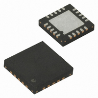
ATTINY84V-10MU Atmel, ATTINY84V-10MU Datasheet - Page 146

ATTINY84V-10MU
Manufacturer Part Number
ATTINY84V-10MU
Description
IC MCU AVR 8K FLASH 10MHZ 20-QFN
Manufacturer
Atmel
Series
AVR® ATtinyr
Specifications of ATTINY84V-10MU
Core Processor
AVR
Core Size
8-Bit
Speed
10MHz
Connectivity
USI
Peripherals
Brown-out Detect/Reset, POR, PWM, Temp Sensor, WDT
Number Of I /o
12
Program Memory Size
8KB (4K x 16)
Program Memory Type
FLASH
Eeprom Size
512 x 8
Ram Size
512 x 8
Voltage - Supply (vcc/vdd)
1.8 V ~ 5.5 V
Data Converters
A/D 8x10b
Oscillator Type
Internal
Operating Temperature
-40°C ~ 85°C
Package / Case
20-MLF®, QFN
Processor Series
ATTINY8x
Core
AVR8
Data Bus Width
8 bit
Data Ram Size
512 B
Interface Type
SPI
Maximum Clock Frequency
10 MHz
Number Of Programmable I/os
12
Number Of Timers
2
Maximum Operating Temperature
+ 85 C
Mounting Style
SMD/SMT
Minimum Operating Temperature
- 40 C
On-chip Adc
8-ch x 10-bit
For Use With
ATSTK600 - DEV KIT FOR AVR/AVR32770-1007 - ISP 4PORT ATMEL AVR MCU SPI/JTAGATAVRISP2 - PROGRAMMER AVR IN SYSTEM
Lead Free Status / RoHS Status
Lead free / RoHS Compliant
- Current page: 146 of 238
- Download datasheet (5Mb)
146
ATtiny24/44/84
done by first turning off the ADC, then changing multiplexer settings and then turn on the ADC.
Alternatively, the first conversion results after changing multiplexer settings should be discarded.
Table 16-4.
Notes:
See
tions of offset calibration channels. MUX0 bit works as a gain selection bit for differential
channels. When MUX0 is cleared (‘0’) 1x gain is selected and when it is set (‘1’) 20x gain is
selected. For normal differential channel pairs MUX5 bit work as a polarity reversal bit. Toggling
of the MUX5 bit exhanges the positive and negative channel other way a round.
Table 16-5.
Single Ended Input
ADC0 (PA0)
ADC1 (PA1)
ADC2 (PA2)
ADC3 (PA3)
ADC4 (PA4)
ADC5 (PA5)
ADC6 (PA6)
ADC7 (PA7)
Reserved for differential channels
0V (AGND)
1.1V (I Ref)
ADC8
Reserved for offset calibration
Reserved for reversal differential channels
Positive Differential Input
ADC0 (PA0)
ADC1 (PA1)
Table 16-5
(3)
1. See
2. After switching to internal voltage reference the ADC requires a settling time of 1ms before
3. See
4. For offset calibration, only. See
measurements are stable. Conversions starting before this may not be reliable. The ADC must
be enabled during the settling time.
(2)
Single-Ended Input channel Selections.
Differential Input channel Selections.
Table 16-5
“Temperature Measurement” on page
for details of selections of differential input channel selections as well as selec-
for details.
(4)
(1)
Negative Differential Input
ADC0 (PA0)
ADC1 (PA1)
ADC3 (PA3)
ADC0 (PA0)
ADC2 (PA2)
ADC3 (PA3)
(1)
Table 16-5 on page 146
(1)
144.
and
“Operation” on page
Gain 1x
001000
001010
101000
001100
001110
N/A
001000 - 011111
100011 - 100111
101000 - 111111
MUX5:0
MUX5:0
000000
000001
000010
000011
000100
000101
000110
000111
100000
100001
100010
8006K–AVR–10/10
Gain 20x
100011
001001
001011
101001
001101
001111
133.
Related parts for ATTINY84V-10MU
Image
Part Number
Description
Manufacturer
Datasheet
Request
R

Part Number:
Description:
MCU AVR 8KB FLASH 10MHZ 14SOIC
Manufacturer:
Atmel
Datasheet:

Part Number:
Description:
MCU AVR 8KB FLASH 10MHZ 20QFN
Manufacturer:
Atmel
Datasheet:

Part Number:
Description:
MCU AVR 8K ISP FLASH 1.8V 14SOIC
Manufacturer:
Atmel
Datasheet:

Part Number:
Description:
AVR MCU, 8K FLASH, 512B RAM, 512B EE
Manufacturer:
Atmel
Datasheet:

Part Number:
Description:
Manufacturer:
Atmel Corporation
Datasheet:

Part Number:
Description:
Manufacturer:
Atmel Corporation
Datasheet:

Part Number:
Description:
IC MCU AVR 8K FLASH 20MHZ 20-QFN
Manufacturer:
Atmel
Datasheet:

Part Number:
Description:
MCU AVR 8K ISP FLASH 2.7V 14SOIC
Manufacturer:
Atmel
Datasheet:

Part Number:
Description:
MCU AVR 8K FLASH 15MHZ 20-QFN
Manufacturer:
Atmel
Datasheet:

Part Number:
Description:
IC MCU AVR 8K FLASH 20MHZ 14-DIP
Manufacturer:
Atmel
Datasheet:

Part Number:
Description:
MCU AVR 8KB FLASH 10MHZ 14SOIC
Manufacturer:
Atmel
Datasheet:

Part Number:
Description:
MCU AVR 8KB FLASH 20MHZ 20QFN
Manufacturer:
Atmel
Datasheet:

Part Number:
Description:
IC, MCU, 8BIT, 2K FLASH, 20SOIC
Manufacturer:
Atmel
Datasheet:

Part Number:
Description:
IC, MCU, 8BIT, 2K FLASH, 20PDIP
Manufacturer:
Atmel
Datasheet:

Part Number:
Description:
IC, MCU, 8BIT, 8K FLASH, 20PDIP
Manufacturer:
Atmel
Datasheet:


