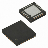
ATTINY84V-10MU Atmel, ATTINY84V-10MU Datasheet - Page 136

ATTINY84V-10MU
Manufacturer Part Number
ATTINY84V-10MU
Description
IC MCU AVR 8K FLASH 10MHZ 20-QFN
Manufacturer
Atmel
Series
AVR® ATtinyr
Specifications of ATTINY84V-10MU
Core Processor
AVR
Core Size
8-Bit
Speed
10MHz
Connectivity
USI
Peripherals
Brown-out Detect/Reset, POR, PWM, Temp Sensor, WDT
Number Of I /o
12
Program Memory Size
8KB (4K x 16)
Program Memory Type
FLASH
Eeprom Size
512 x 8
Ram Size
512 x 8
Voltage - Supply (vcc/vdd)
1.8 V ~ 5.5 V
Data Converters
A/D 8x10b
Oscillator Type
Internal
Operating Temperature
-40°C ~ 85°C
Package / Case
20-MLF®, QFN
Processor Series
ATTINY8x
Core
AVR8
Data Bus Width
8 bit
Data Ram Size
512 B
Interface Type
SPI
Maximum Clock Frequency
10 MHz
Number Of Programmable I/os
12
Number Of Timers
2
Maximum Operating Temperature
+ 85 C
Mounting Style
SMD/SMT
Minimum Operating Temperature
- 40 C
On-chip Adc
8-ch x 10-bit
For Use With
ATSTK600 - DEV KIT FOR AVR/AVR32770-1007 - ISP 4PORT ATMEL AVR MCU SPI/JTAGATAVRISP2 - PROGRAMMER AVR IN SYSTEM
Lead Free Status / RoHS Status
Lead free / RoHS Compliant
- Current page: 136 of 238
- Download datasheet (5Mb)
136
ATtiny24/44/84
The ADC module contains a prescaler, as illustrated in
ates an acceptable ADC clock frequency from any CPU frequency above 100 kHz. The
prescaling is set by the ADPS bits in ADCSRA. The prescaler starts counting from the moment
the ADC is switched on by setting the ADEN bit in ADCSRA. The prescaler keeps running for as
long as the ADEN bit is set, and is continuously reset when ADEN is low.
When initiating a single ended conversion by setting the ADSC bit in ADCSRA, the conversion
starts at the following rising edge of the ADC clock cycle.
A normal conversion takes 13 ADC clock cycles. The first conversion after the ADC is switched
on (ADEN in ADCSRA is set) takes 25 ADC clock cycles in order to initialize the analog circuitry,
as shown in
Figure 16-4. ADC Timing Diagram, First Conversion (Single Conversion Mode)
The actual sample-and-hold takes place 1.5 ADC clock cycles after the start of a normal conver-
sion and 13.5 ADC clock cycles after the start of an first conversion. When a conversion is
complete, the result is written to the ADC Data Registers, and ADIF is set. In Single Conversion
mode, ADSC is cleared simultaneously. The software may then set ADSC again, and a new
conversion will be initiated on the first rising ADC clock edge.
Figure 16-5. ADC Timing Diagram, Single Conversion
Cycle Number
ADC Clock
ADEN
ADSC
ADIF
ADCH
ADCL
Cycle Number
ADC Clock
ADSC
ADIF
ADCH
ADCL
Figure 16-4
1
1
2
MUX and REFS
Update
2
MUX and REFS
Update
below.
12
3
13
Sample & Hold
4
14
5
15
6
Sample & Hold
16
First Conversion
17
7
One Conversion
18
8
19
9
20
Figure 16-3 on page
10
Conversion
Complete
21
11
22
Conversion
Complete
23
12
24
13
25
Sign and MSB of Result
Sign and MSB of Result
135, which gener-
LSB of Result
Next Conversion
1
Next
Conversion
1
LSB of Result
8006K–AVR–10/10
2
MUX and REFS
Update
2
MUX and REFS
Update
3
3
Related parts for ATTINY84V-10MU
Image
Part Number
Description
Manufacturer
Datasheet
Request
R

Part Number:
Description:
MCU AVR 8KB FLASH 10MHZ 14SOIC
Manufacturer:
Atmel
Datasheet:

Part Number:
Description:
MCU AVR 8KB FLASH 10MHZ 20QFN
Manufacturer:
Atmel
Datasheet:

Part Number:
Description:
MCU AVR 8K ISP FLASH 1.8V 14SOIC
Manufacturer:
Atmel
Datasheet:

Part Number:
Description:
AVR MCU, 8K FLASH, 512B RAM, 512B EE
Manufacturer:
Atmel
Datasheet:

Part Number:
Description:
Manufacturer:
Atmel Corporation
Datasheet:

Part Number:
Description:
Manufacturer:
Atmel Corporation
Datasheet:

Part Number:
Description:
IC MCU AVR 8K FLASH 20MHZ 20-QFN
Manufacturer:
Atmel
Datasheet:

Part Number:
Description:
MCU AVR 8K ISP FLASH 2.7V 14SOIC
Manufacturer:
Atmel
Datasheet:

Part Number:
Description:
MCU AVR 8K FLASH 15MHZ 20-QFN
Manufacturer:
Atmel
Datasheet:

Part Number:
Description:
IC MCU AVR 8K FLASH 20MHZ 14-DIP
Manufacturer:
Atmel
Datasheet:

Part Number:
Description:
MCU AVR 8KB FLASH 10MHZ 14SOIC
Manufacturer:
Atmel
Datasheet:

Part Number:
Description:
MCU AVR 8KB FLASH 20MHZ 20QFN
Manufacturer:
Atmel
Datasheet:

Part Number:
Description:
IC, MCU, 8BIT, 2K FLASH, 20SOIC
Manufacturer:
Atmel
Datasheet:

Part Number:
Description:
IC, MCU, 8BIT, 2K FLASH, 20PDIP
Manufacturer:
Atmel
Datasheet:

Part Number:
Description:
IC, MCU, 8BIT, 8K FLASH, 20PDIP
Manufacturer:
Atmel
Datasheet:


