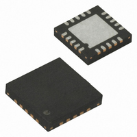
ATTINY84V-10MU Atmel, ATTINY84V-10MU Datasheet - Page 165

ATTINY84V-10MU
Manufacturer Part Number
ATTINY84V-10MU
Description
IC MCU AVR 8K FLASH 10MHZ 20-QFN
Manufacturer
Atmel
Series
AVR® ATtinyr
Specifications of ATTINY84V-10MU
Core Processor
AVR
Core Size
8-Bit
Speed
10MHz
Connectivity
USI
Peripherals
Brown-out Detect/Reset, POR, PWM, Temp Sensor, WDT
Number Of I /o
12
Program Memory Size
8KB (4K x 16)
Program Memory Type
FLASH
Eeprom Size
512 x 8
Ram Size
512 x 8
Voltage - Supply (vcc/vdd)
1.8 V ~ 5.5 V
Data Converters
A/D 8x10b
Oscillator Type
Internal
Operating Temperature
-40°C ~ 85°C
Package / Case
20-MLF®, QFN
Processor Series
ATTINY8x
Core
AVR8
Data Bus Width
8 bit
Data Ram Size
512 B
Interface Type
SPI
Maximum Clock Frequency
10 MHz
Number Of Programmable I/os
12
Number Of Timers
2
Maximum Operating Temperature
+ 85 C
Mounting Style
SMD/SMT
Minimum Operating Temperature
- 40 C
On-chip Adc
8-ch x 10-bit
For Use With
ATSTK600 - DEV KIT FOR AVR/AVR32770-1007 - ISP 4PORT ATMEL AVR MCU SPI/JTAGATAVRISP2 - PROGRAMMER AVR IN SYSTEM
Lead Free Status / RoHS Status
Lead free / RoHS Compliant
- Current page: 165 of 238
- Download datasheet (5Mb)
19.5.2
Table 19-12. Serial Programming Instruction Set
8006K–AVR–10/10
Instruction/Operation
Programming Enable
Chip Erase (Program Memory/EEPROM)
Poll RDY/BSY
Load Instructions
Load Extended Address byte
Load Program Memory Page, High byte
Load Program Memory Page, Low byte
Load EEPROM Memory Page (page access)
Read Instructions
Read Program Memory, High byte
Read Program Memory, Low byte
Read EEPROM Memory
Read Lock bits
Read Signature Byte
Read Fuse bits
Read Fuse High bits
Read Extended Fuse Bits
Read Calibration Byte
Serial Programming Instruction set
(1)
Table 19-11. Minimum Wait Delay Before Writing the Next Flash or EEPROM Location
The instruction set is described in
Symbol
t
t
t
t
6. Any memory location can be verified by using the Read instruction which returns the
7. At the end of the programming session, RESET can be set high to commence normal
8. Power-off sequence (if needed):
WD_FLASH
WD_EEPROM
WD_ERASE
WD_FUSE
next page (See
file(s) need to be programmed.
content at the selected address at serial output MISO.
operation.
Set RESET to “1”.
Turn V
CC
power off.
Table 19-11 on page
Byte 1
$AC
$AC
$4D
$C1
$A0
$F0
$48
$40
$28
$20
$58
$30
$50
$58
$50
$38
Table 19-12
adr MSB
adr MSB
adr MSB
adr MSB
165). In a chip erased device, no 0xFF in the data
Byte 2
$53
$80
$00
$00
$00
$00
$00
$00
$00
$08
$08
$00
and
Instruction Format
Figure 19-2 on page
Minimum Wait Delay
Extended adr
4.5 ms
4.0 ms
9.0 ms
4.5 ms
adr LSB
adr LSB
adr LSB
adr LSB
adr LSB
adr LSB
adr LSB
Byte 3
$00
$00
$00
$00
$00
$00
$00
$00
ATtiny24/44/84
166.
high data byte out
low data byte out
high data byte in
low data byte in
data byte out
data byte out
data byte out
data byte out
data byte out
data byte out
data byte out
data byte out
data byte in
Byte4
$00
$00
$00
165
Related parts for ATTINY84V-10MU
Image
Part Number
Description
Manufacturer
Datasheet
Request
R

Part Number:
Description:
MCU AVR 8KB FLASH 10MHZ 14SOIC
Manufacturer:
Atmel
Datasheet:

Part Number:
Description:
MCU AVR 8KB FLASH 10MHZ 20QFN
Manufacturer:
Atmel
Datasheet:

Part Number:
Description:
MCU AVR 8K ISP FLASH 1.8V 14SOIC
Manufacturer:
Atmel
Datasheet:

Part Number:
Description:
AVR MCU, 8K FLASH, 512B RAM, 512B EE
Manufacturer:
Atmel
Datasheet:

Part Number:
Description:
Manufacturer:
Atmel Corporation
Datasheet:

Part Number:
Description:
Manufacturer:
Atmel Corporation
Datasheet:

Part Number:
Description:
IC MCU AVR 8K FLASH 20MHZ 20-QFN
Manufacturer:
Atmel
Datasheet:

Part Number:
Description:
MCU AVR 8K ISP FLASH 2.7V 14SOIC
Manufacturer:
Atmel
Datasheet:

Part Number:
Description:
MCU AVR 8K FLASH 15MHZ 20-QFN
Manufacturer:
Atmel
Datasheet:

Part Number:
Description:
IC MCU AVR 8K FLASH 20MHZ 14-DIP
Manufacturer:
Atmel
Datasheet:

Part Number:
Description:
MCU AVR 8KB FLASH 10MHZ 14SOIC
Manufacturer:
Atmel
Datasheet:

Part Number:
Description:
MCU AVR 8KB FLASH 20MHZ 20QFN
Manufacturer:
Atmel
Datasheet:

Part Number:
Description:
IC, MCU, 8BIT, 2K FLASH, 20SOIC
Manufacturer:
Atmel
Datasheet:

Part Number:
Description:
IC, MCU, 8BIT, 2K FLASH, 20PDIP
Manufacturer:
Atmel
Datasheet:

Part Number:
Description:
IC, MCU, 8BIT, 8K FLASH, 20PDIP
Manufacturer:
Atmel
Datasheet:


