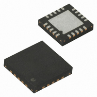
ATTINY84V-10MU Atmel, ATTINY84V-10MU Datasheet - Page 30

ATTINY84V-10MU
Manufacturer Part Number
ATTINY84V-10MU
Description
IC MCU AVR 8K FLASH 10MHZ 20-QFN
Manufacturer
Atmel
Series
AVR® ATtinyr
Specifications of ATTINY84V-10MU
Core Processor
AVR
Core Size
8-Bit
Speed
10MHz
Connectivity
USI
Peripherals
Brown-out Detect/Reset, POR, PWM, Temp Sensor, WDT
Number Of I /o
12
Program Memory Size
8KB (4K x 16)
Program Memory Type
FLASH
Eeprom Size
512 x 8
Ram Size
512 x 8
Voltage - Supply (vcc/vdd)
1.8 V ~ 5.5 V
Data Converters
A/D 8x10b
Oscillator Type
Internal
Operating Temperature
-40°C ~ 85°C
Package / Case
20-MLF®, QFN
Processor Series
ATTINY8x
Core
AVR8
Data Bus Width
8 bit
Data Ram Size
512 B
Interface Type
SPI
Maximum Clock Frequency
10 MHz
Number Of Programmable I/os
12
Number Of Timers
2
Maximum Operating Temperature
+ 85 C
Mounting Style
SMD/SMT
Minimum Operating Temperature
- 40 C
On-chip Adc
8-ch x 10-bit
For Use With
ATSTK600 - DEV KIT FOR AVR/AVR32770-1007 - ISP 4PORT ATMEL AVR MCU SPI/JTAGATAVRISP2 - PROGRAMMER AVR IN SYSTEM
Lead Free Status / RoHS Status
Lead free / RoHS Compliant
- Current page: 30 of 238
- Download datasheet (5Mb)
6.2.6
6.3
6.3.1
6.4
6.5
6.5.1
30
System Clock Prescaler
Clock Output Buffer
Register Description
ATtiny24/44/84
Default Clock Source
Switching Time
OSCCAL – Oscillator Calibration Register
The device is shipped with CKSEL = “0010”, SUT = “10”, and CKDIV8 programmed. The default
clock source setting is therefore the Internal Oscillator running at 8.0 MHz with longest start-up
time and an initial system clock prescaling of 8, resulting in 1.0 MHz system clock. This default
setting ensures that all users can make their desired clock source setting using an in-system or
high-voltage programmer.
For low-voltage devices (ATtiny24V/44V/84V) it should be noted that unprogramming the
CKDIV8 fuse may result in overclocking. At low voltages (below 2.7V) the devices are rated for
maximum 4 MHz operation (see
internal oscillator directly to the system clock line will run the device at 8 MHz.
The ATtiny24/44/84 system clock can be divided by setting the
ter” on page
requirement for processing power is low. This can be used with all clock source options, and it
will affect the clock frequency of the CPU and all synchronous peripherals. clk
and clk
When switching between prescaler settings, the System Clock Prescaler ensures that no
glitches occur in the clock system and that no intermediate frequency is higher than neither the
clock frequency corresponding to the previous setting, nor the clock frequency corresponding to
the new setting.
The ripple counter that implements the prescaler runs at the frequency of the undivided clock,
which may be faster than the CPU’s clock frequency. Hence, it is not possible to determine the
state of the prescaler – even if it were readable, and the exact time it takes to switch from one
clock division to another cannot be exactly predicted.
From the time the CLKPS values are written, it takes between T1 + T2 and T1 + 2*T2 before the
new clock frequency is active. In this interval, 2 active clock edges are produced. Here, T1 is the
previous clock period, and T2 is the period corresponding to the new prescaler setting.
The device can output the system clock on the CKOUT pin. To enable the output, the CKOUT
fuse has to be programmed. This mode is suitable when the chip clock is used to drive other cir-
cuits on the system. Note that the clock will not be output during reset and that the normal
operation of the I/O pin will be overridden when the fuse is programmed. Any clock source,
including the internal RC Oscillator, can be selected when the clock is output on CKOUT. If the
System Clock Prescaler is used, it is the divided system clock that is output.
• Bits 7:0 – CAL7:0: Oscillator Calibration Value
Bit
0x31 (0x51)
Read/Write
Initial Value
FLASH
are divided by a factor as shown in
31. This feature can be used to decrease power consumption when the
CAL7
R/W
7
CAL6
R/W
6
Section 20.3 on page
Device Specific Calibration Value
CAL5
R/W
5
CAL4
R/W
4
Table 6-11 on page
CAL3
R/W
3
175), but routing the clock signal from the
CAL2
R/W
2
“CLKPR – Clock Prescale Regis-
32.
CAL1
R/W
1
I/O
CAL0
R/W
, clk
0
8006K–AVR–10/10
ADC
OSCCAL
, clk
CPU
,
Related parts for ATTINY84V-10MU
Image
Part Number
Description
Manufacturer
Datasheet
Request
R

Part Number:
Description:
MCU AVR 8KB FLASH 10MHZ 14SOIC
Manufacturer:
Atmel
Datasheet:

Part Number:
Description:
MCU AVR 8KB FLASH 10MHZ 20QFN
Manufacturer:
Atmel
Datasheet:

Part Number:
Description:
MCU AVR 8K ISP FLASH 1.8V 14SOIC
Manufacturer:
Atmel
Datasheet:

Part Number:
Description:
AVR MCU, 8K FLASH, 512B RAM, 512B EE
Manufacturer:
Atmel
Datasheet:

Part Number:
Description:
Manufacturer:
Atmel Corporation
Datasheet:

Part Number:
Description:
Manufacturer:
Atmel Corporation
Datasheet:

Part Number:
Description:
IC MCU AVR 8K FLASH 20MHZ 20-QFN
Manufacturer:
Atmel
Datasheet:

Part Number:
Description:
MCU AVR 8K ISP FLASH 2.7V 14SOIC
Manufacturer:
Atmel
Datasheet:

Part Number:
Description:
MCU AVR 8K FLASH 15MHZ 20-QFN
Manufacturer:
Atmel
Datasheet:

Part Number:
Description:
IC MCU AVR 8K FLASH 20MHZ 14-DIP
Manufacturer:
Atmel
Datasheet:

Part Number:
Description:
MCU AVR 8KB FLASH 10MHZ 14SOIC
Manufacturer:
Atmel
Datasheet:

Part Number:
Description:
MCU AVR 8KB FLASH 20MHZ 20QFN
Manufacturer:
Atmel
Datasheet:

Part Number:
Description:
IC, MCU, 8BIT, 2K FLASH, 20SOIC
Manufacturer:
Atmel
Datasheet:

Part Number:
Description:
IC, MCU, 8BIT, 2K FLASH, 20PDIP
Manufacturer:
Atmel
Datasheet:

Part Number:
Description:
IC, MCU, 8BIT, 8K FLASH, 20PDIP
Manufacturer:
Atmel
Datasheet:


