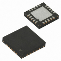
ATTINY84V-10MU Atmel, ATTINY84V-10MU Datasheet - Page 25

ATTINY84V-10MU
Manufacturer Part Number
ATTINY84V-10MU
Description
IC MCU AVR 8K FLASH 10MHZ 20-QFN
Manufacturer
Atmel
Series
AVR® ATtinyr
Specifications of ATTINY84V-10MU
Core Processor
AVR
Core Size
8-Bit
Speed
10MHz
Connectivity
USI
Peripherals
Brown-out Detect/Reset, POR, PWM, Temp Sensor, WDT
Number Of I /o
12
Program Memory Size
8KB (4K x 16)
Program Memory Type
FLASH
Eeprom Size
512 x 8
Ram Size
512 x 8
Voltage - Supply (vcc/vdd)
1.8 V ~ 5.5 V
Data Converters
A/D 8x10b
Oscillator Type
Internal
Operating Temperature
-40°C ~ 85°C
Package / Case
20-MLF®, QFN
Processor Series
ATTINY8x
Core
AVR8
Data Bus Width
8 bit
Data Ram Size
512 B
Interface Type
SPI
Maximum Clock Frequency
10 MHz
Number Of Programmable I/os
12
Number Of Timers
2
Maximum Operating Temperature
+ 85 C
Mounting Style
SMD/SMT
Minimum Operating Temperature
- 40 C
On-chip Adc
8-ch x 10-bit
For Use With
ATSTK600 - DEV KIT FOR AVR/AVR32770-1007 - ISP 4PORT ATMEL AVR MCU SPI/JTAGATAVRISP2 - PROGRAMMER AVR IN SYSTEM
Lead Free Status / RoHS Status
Lead free / RoHS Compliant
- Current page: 25 of 238
- Download datasheet (5Mb)
6.1.2
6.1.3
6.1.4
6.2
8006K–AVR–10/10
Clock Sources
I/O Clock – clk
Flash Clock – clk
ADC Clock – clk
I/O
The I/O clock is used by the majority of the I/O modules, like Timer/Counter. The I/O clock is
also used by the External Interrupt module, but note that some external interrupts are detected
by asynchronous logic, allowing such interrupts to be detected even if the I/O clock is halted.
The Flash clock controls operation of the Flash interface. The Flash clock is usually active simul-
taneously with the CPU clock.
The ADC is provided with a dedicated clock domain. This allows halting the CPU and I/O clocks
in order to reduce noise generated by digital circuitry. This gives more accurate ADC conversion
results.
The device has the following clock source options, selectable by Flash Fuse bits as shown
below. The clock from the selected source is input to the AVR clock generator, and routed to the
appropriate modules.
Table 6-1.
Note:
The various choices for each clocking option is given in the following sections. When the CPU
wakes up from Power-down the selected clock source is used to time the start-up, ensuring sta-
ble Oscillator operation before instruction execution starts. When the CPU starts from reset,
there is an additional delay allowing the power to reach a stable level before commencing nor-
mal operation. The Watchdog Oscillator is used for timing this real-time part of the start-up time.
The number of WDT Oscillator cycles used for each time-out is shown in
Table 6-2.
ADC
Device Clocking Option
External Clock (see
Reserved
Calibrated Internal 8 MHz Oscillator (see
Reserved
Internal 128 kHz Oscillator (see
Reserved
Low-Frequency Crystal Oscillator (see
Reserved
Crystal Oscillator / Ceramic Resonator (see
FLASH
1. For all fuses “1” means unprogrammed and “0” means programmed.
Typ Time-out
Device Clocking Options Select
Number of Watchdog Oscillator Cycles
64 ms
4 ms
page
26)
page
27)
page
page
page
28)
26)
28)
Number of Cycles
8K (8,192)
512
ATtiny24/44/84
Table
CKSEL3:0
1000-1111
6-2.
0000
0001
0010
0011
0100
0101
0110
0111
(1)
25
Related parts for ATTINY84V-10MU
Image
Part Number
Description
Manufacturer
Datasheet
Request
R

Part Number:
Description:
MCU AVR 8KB FLASH 10MHZ 14SOIC
Manufacturer:
Atmel
Datasheet:

Part Number:
Description:
MCU AVR 8KB FLASH 10MHZ 20QFN
Manufacturer:
Atmel
Datasheet:

Part Number:
Description:
MCU AVR 8K ISP FLASH 1.8V 14SOIC
Manufacturer:
Atmel
Datasheet:

Part Number:
Description:
AVR MCU, 8K FLASH, 512B RAM, 512B EE
Manufacturer:
Atmel
Datasheet:

Part Number:
Description:
Manufacturer:
Atmel Corporation
Datasheet:

Part Number:
Description:
Manufacturer:
Atmel Corporation
Datasheet:

Part Number:
Description:
IC MCU AVR 8K FLASH 20MHZ 20-QFN
Manufacturer:
Atmel
Datasheet:

Part Number:
Description:
MCU AVR 8K ISP FLASH 2.7V 14SOIC
Manufacturer:
Atmel
Datasheet:

Part Number:
Description:
MCU AVR 8K FLASH 15MHZ 20-QFN
Manufacturer:
Atmel
Datasheet:

Part Number:
Description:
IC MCU AVR 8K FLASH 20MHZ 14-DIP
Manufacturer:
Atmel
Datasheet:

Part Number:
Description:
MCU AVR 8KB FLASH 10MHZ 14SOIC
Manufacturer:
Atmel
Datasheet:

Part Number:
Description:
MCU AVR 8KB FLASH 20MHZ 20QFN
Manufacturer:
Atmel
Datasheet:

Part Number:
Description:
IC, MCU, 8BIT, 2K FLASH, 20SOIC
Manufacturer:
Atmel
Datasheet:

Part Number:
Description:
IC, MCU, 8BIT, 2K FLASH, 20PDIP
Manufacturer:
Atmel
Datasheet:

Part Number:
Description:
IC, MCU, 8BIT, 8K FLASH, 20PDIP
Manufacturer:
Atmel
Datasheet:


