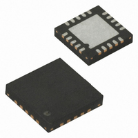
ATTINY84V-10MU Atmel, ATTINY84V-10MU Datasheet - Page 66

ATTINY84V-10MU
Manufacturer Part Number
ATTINY84V-10MU
Description
IC MCU AVR 8K FLASH 10MHZ 20-QFN
Manufacturer
Atmel
Series
AVR® ATtinyr
Specifications of ATTINY84V-10MU
Core Processor
AVR
Core Size
8-Bit
Speed
10MHz
Connectivity
USI
Peripherals
Brown-out Detect/Reset, POR, PWM, Temp Sensor, WDT
Number Of I /o
12
Program Memory Size
8KB (4K x 16)
Program Memory Type
FLASH
Eeprom Size
512 x 8
Ram Size
512 x 8
Voltage - Supply (vcc/vdd)
1.8 V ~ 5.5 V
Data Converters
A/D 8x10b
Oscillator Type
Internal
Operating Temperature
-40°C ~ 85°C
Package / Case
20-MLF®, QFN
Processor Series
ATTINY8x
Core
AVR8
Data Bus Width
8 bit
Data Ram Size
512 B
Interface Type
SPI
Maximum Clock Frequency
10 MHz
Number Of Programmable I/os
12
Number Of Timers
2
Maximum Operating Temperature
+ 85 C
Mounting Style
SMD/SMT
Minimum Operating Temperature
- 40 C
On-chip Adc
8-ch x 10-bit
For Use With
ATSTK600 - DEV KIT FOR AVR/AVR32770-1007 - ISP 4PORT ATMEL AVR MCU SPI/JTAGATAVRISP2 - PROGRAMMER AVR IN SYSTEM
Lead Free Status / RoHS Status
Lead free / RoHS Compliant
- Current page: 66 of 238
- Download datasheet (5Mb)
66
ATtiny24/44/84
• Port B, Bit 3 – RESET/dW/PCINT11
Table 10-8 on page 66
overriding signals shown in
Table 10-8.
1.
2.
Signal
Name
PUOE
PUOV
DDOE
DDOV
PVOE
PVOV
PTOE
DIEOE
DIEOV
DI
AIO
• RESET: External Reset input is active low and enabled by unprogramming (“1”) the
• dW: When the debugWIRE Enable (DWEN) Fuse is programmed and Lock bits are
• PCINT11: Pin Change Interrupt source 11. The PB3 pin can serve as an external interrupt
RSTDISBL Fuse. Pullup is activated and output driver and digital input are deactivated when
the pin is used as the RESET pin.
unprogrammed, the debugWIRE system within the target device is activated. The RESET
port pin is configured as a wire-AND (open-drain) bi-directional I/O pin with pull-up enabled
and becomes the communication gateway between target and emulator.
source for pin change interrupt 1.
RSTDISBL is 1 when the Fuse is “0” (Programmed).
DebugWIRE is enabled wheb DWEN Fuse is programmed and Lock bits are unprogrammed.
PB3/
PCINT11
RSTDISBL
1
RSTDISBL
DEBUGWIRE_ENABLE
Transmit
RSTDISBL
0
0
RSTDISBL
PCINT11 • PCIE1
DEBUGWIRE_ENABLE
PCINT11 • PCIE1)
dW/PCINT11 Input
Overriding Signals for Alternate Functions in PB3:PB2
RESET/dW/
(1)
(1)
(1)
(1)
and
+ DEBUGWIRE_ENABLE
+ DEBUGWIRE_ENABLE
+ DEBUGWIRE_ENABLE
+ DEBUGWIRE_ENABLE
Figure 10-5 on page
Table 10-9 on page 67
(2)
(2)
+ (RSTDISBL
• debugWire
(2)
(2)
(2)
(2)
(1)
59.
+
•
relate the alternate functions of Port B to the
PB2/INT0/OC0A/CKOUT/PCINT10
CKOUT
0
CKOUT
1
CKOUT + OC0A enable
CKOUT • System Clock + CKOUT • OC0A
0
PCINT10 • PCIE1 + INT0
PCINT10 • PCIE1 + INT0
INT0/PCINT10 Input
8006K–AVR–10/10
Related parts for ATTINY84V-10MU
Image
Part Number
Description
Manufacturer
Datasheet
Request
R

Part Number:
Description:
MCU AVR 8KB FLASH 10MHZ 14SOIC
Manufacturer:
Atmel
Datasheet:

Part Number:
Description:
MCU AVR 8KB FLASH 10MHZ 20QFN
Manufacturer:
Atmel
Datasheet:

Part Number:
Description:
MCU AVR 8K ISP FLASH 1.8V 14SOIC
Manufacturer:
Atmel
Datasheet:

Part Number:
Description:
AVR MCU, 8K FLASH, 512B RAM, 512B EE
Manufacturer:
Atmel
Datasheet:

Part Number:
Description:
Manufacturer:
Atmel Corporation
Datasheet:

Part Number:
Description:
Manufacturer:
Atmel Corporation
Datasheet:

Part Number:
Description:
IC MCU AVR 8K FLASH 20MHZ 20-QFN
Manufacturer:
Atmel
Datasheet:

Part Number:
Description:
MCU AVR 8K ISP FLASH 2.7V 14SOIC
Manufacturer:
Atmel
Datasheet:

Part Number:
Description:
MCU AVR 8K FLASH 15MHZ 20-QFN
Manufacturer:
Atmel
Datasheet:

Part Number:
Description:
IC MCU AVR 8K FLASH 20MHZ 14-DIP
Manufacturer:
Atmel
Datasheet:

Part Number:
Description:
MCU AVR 8KB FLASH 10MHZ 14SOIC
Manufacturer:
Atmel
Datasheet:

Part Number:
Description:
MCU AVR 8KB FLASH 20MHZ 20QFN
Manufacturer:
Atmel
Datasheet:

Part Number:
Description:
IC, MCU, 8BIT, 2K FLASH, 20SOIC
Manufacturer:
Atmel
Datasheet:

Part Number:
Description:
IC, MCU, 8BIT, 2K FLASH, 20PDIP
Manufacturer:
Atmel
Datasheet:

Part Number:
Description:
IC, MCU, 8BIT, 8K FLASH, 20PDIP
Manufacturer:
Atmel
Datasheet:


