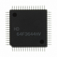
HD64F3644DV Renesas Electronics America, HD64F3644DV Datasheet - Page 149

HD64F3644DV
Manufacturer Part Number
HD64F3644DV
Description
IC H8/3644 MCU FLASH 64QFP
Manufacturer
Renesas Electronics America
Series
H8® H8/300Lr
Datasheet
1.HD64F3644HV.pdf
(551 pages)
Specifications of HD64F3644DV
Core Processor
H8/300L
Core Size
8-Bit
Speed
8MHz
Connectivity
SCI
Peripherals
PWM, WDT
Number Of I /o
53
Program Memory Size
32KB (32K x 8)
Program Memory Type
FLASH
Ram Size
1K x 8
Voltage - Supply (vcc/vdd)
2.7 V ~ 5.5 V
Data Converters
A/D 8x8b
Oscillator Type
Internal
Operating Temperature
-40°C ~ 85°C
Package / Case
64-QFP
Lead Free Status / RoHS Status
Lead free / RoHS Compliant
Eeprom Size
-
Available stocks
Company
Part Number
Manufacturer
Quantity
Price
Company:
Part Number:
HD64F3644DV
Manufacturer:
Renesas Electronics America
Quantity:
10 000
- Current page: 149 of 551
- Download datasheet (4Mb)
6.7
The on-chip flash memory of the H8/3644F, H8/3643F, and H8/3642AF is programmed and
erased by software, using the CPU. There are five flash memory operating modes: program mode,
erase mode, program-verify mode, erase-verify mode, and prewrite-verify mode. Transitions to
these modes can be made by setting the P, E, PV, and EV bits in the flash memory control register
(FLMCR).
The flash memory cannot be read while being programmed or erased. Therefore, the program that
controls flash memory programming and erasing should be located and executed in on-chip RAM
or external memory. A description of each mode is given below, with recommended flowcharts
and sample programs for programming and erasing.
See section 6.9, Flash Memory Programming and Erasing Precautions, for additional notes on
programming and erasing.
6.7.1
To write data into the flash memory, follow the programming algorithm shown in figure 6.13. This
programming algorithm enables data to be written without subjecting the device to voltage stress
or impairing the reliability of the programmed data.
To write data, first set the blocks to be programmed with erase block registers 1 and 2 (EBR1,
EBR2), and write the data to the address to be programmed, as in writing to RAM. The flash
memory latches the programming address and programming data in an address latch and data
latch. Next set the P bit in FLMCR, selecting program mode. The programming time is the time
during which the P bit is set. Make a setting so that the total programming time does not exceed 1
ms. Programming for too long a time, due to program runaway for example, can damage the
device. Before selecting program mode, set up the watchdog timer so as to prevent
overprogramming.
For details of the programming procedure, see section 6.7.3, Programming Flowchart and Sample
Program.
Programming and Erasing Flash Memory
Program Mode
Rev. 6.00 Sep 12, 2006 page 127 of 526
REJ09B0326-0600
Section 6 ROM
Related parts for HD64F3644DV
Image
Part Number
Description
Manufacturer
Datasheet
Request
R

Part Number:
Description:
(HD64 Series) Hitachi Single-Chip Microcomputer
Manufacturer:
Hitachi Semiconductor
Datasheet:

Part Number:
Description:
KIT STARTER FOR M16C/29
Manufacturer:
Renesas Electronics America
Datasheet:

Part Number:
Description:
KIT STARTER FOR R8C/2D
Manufacturer:
Renesas Electronics America
Datasheet:

Part Number:
Description:
R0K33062P STARTER KIT
Manufacturer:
Renesas Electronics America
Datasheet:

Part Number:
Description:
KIT STARTER FOR R8C/23 E8A
Manufacturer:
Renesas Electronics America
Datasheet:

Part Number:
Description:
KIT STARTER FOR R8C/25
Manufacturer:
Renesas Electronics America
Datasheet:

Part Number:
Description:
KIT STARTER H8S2456 SHARPE DSPLY
Manufacturer:
Renesas Electronics America
Datasheet:

Part Number:
Description:
KIT STARTER FOR R8C38C
Manufacturer:
Renesas Electronics America
Datasheet:

Part Number:
Description:
KIT STARTER FOR R8C35C
Manufacturer:
Renesas Electronics America
Datasheet:

Part Number:
Description:
KIT STARTER FOR R8CL3AC+LCD APPS
Manufacturer:
Renesas Electronics America
Datasheet:

Part Number:
Description:
KIT STARTER FOR RX610
Manufacturer:
Renesas Electronics America
Datasheet:

Part Number:
Description:
KIT STARTER FOR R32C/118
Manufacturer:
Renesas Electronics America
Datasheet:

Part Number:
Description:
KIT DEV RSK-R8C/26-29
Manufacturer:
Renesas Electronics America
Datasheet:

Part Number:
Description:
KIT STARTER FOR SH7124
Manufacturer:
Renesas Electronics America
Datasheet:

Part Number:
Description:
KIT STARTER FOR H8SX/1622
Manufacturer:
Renesas Electronics America
Datasheet:


