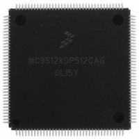
MC9S12XDP512CAG Freescale Semiconductor, MC9S12XDP512CAG Datasheet - Page 56

MC9S12XDP512CAG
Manufacturer Part Number
MC9S12XDP512CAG
Description
IC MCU 512K FLASH 144-LQFP
Manufacturer
Freescale Semiconductor
Series
HCS12r
Datasheet
1.MC9S12XD64CAA.pdf
(1348 pages)
Specifications of MC9S12XDP512CAG
Core Processor
HCS12X
Core Size
16-Bit
Speed
80MHz
Connectivity
CAN, EBI/EMI, I²C, IrDA, LIN, SCI, SPI
Peripherals
LVD, POR, PWM, WDT
Number Of I /o
119
Program Memory Size
512KB (512K x 8)
Program Memory Type
FLASH
Eeprom Size
4K x 8
Ram Size
32K x 8
Voltage - Supply (vcc/vdd)
2.35 V ~ 5.5 V
Data Converters
A/D 24x10b
Oscillator Type
External
Operating Temperature
-40°C ~ 85°C
Package / Case
144-LQFP
Processor Series
S12XD
Core
HCS12
Data Bus Width
16 bit
Data Ram Size
32 KB
Interface Type
CAN/I2C/SCI/SPI
Maximum Clock Frequency
40 MHz
Number Of Programmable I/os
119
Number Of Timers
12
Maximum Operating Temperature
+ 85 C
Mounting Style
SMD/SMT
3rd Party Development Tools
EWHCS12
Development Tools By Supplier
EVB9S12XDP512E
Minimum Operating Temperature
- 40 C
On-chip Adc
2 (24-ch x 10-bit)
Cpu Family
HCS12
Device Core Size
16b
Frequency (max)
40MHz
Total Internal Ram Size
32KB
# I/os (max)
119
Number Of Timers - General Purpose
12
Operating Supply Voltage (typ)
2.5/5V
Operating Supply Voltage (max)
2.75/5.5V
Operating Supply Voltage (min)
2.35/3.15V
Instruction Set Architecture
CISC
Operating Temp Range
-40C to 85C
Operating Temperature Classification
Industrial
Mounting
Surface Mount
Pin Count
144
Package Type
LQFP
For Use With
DEMO9S12XDT512E - BOARD DEMO FOR MC9S12XDT512EVB9S12XDP512E - BOARD DEMO FOR MC9S12XDP512
Lead Free Status / RoHS Status
Lead free / RoHS Compliant
Available stocks
Company
Part Number
Manufacturer
Quantity
Price
Company:
Part Number:
MC9S12XDP512CAG
Manufacturer:
Freescale Semiconductor
Quantity:
10 000
Part Number:
MC9S12XDP512CAG
Manufacturer:
FREESCLA
Quantity:
20 000
- Current page: 56 of 1348
- Download datasheet (8Mb)
Chapter 1 Device Overview MC9S12XD-Family
1.2.3.3
This input only pin is reserved for test. This pin has a pulldown device.
1.2.3.4
This input only pin enables or disables the on-chip voltage regulator. The input has a pullup device.
1.2.3.5
Please ask your Freescale representative for the interactive application note to compute PLL loop filter
elements. Any current leakage on this pin must be avoided.
1.2.3.6
The BKGD/MODC pin is used as a pseudo-open-drain pin for the background debug communication. It
is used as a MCU operating mode select pin during reset. The state of this pin is latched to the MODC bit
at the rising edge of RESET. The BKGD pin has a pullup device.
1.2.3.7
PAD[23:8] are general-purpose input or output pins and analog inputs AN[23:8] of the analog-to-digital
converter ATD1.
1.2.3.8
PAD[7:0] are general-purpose input or output pins and analog inputs AN[7:0] of the analog-to-digital
converter ATD0.
1.2.3.9
PAD[15:0] are general-purpose input or output pins and analog inputs AN[15:0] of the analog-to-digital
converter ATD1.
56
TEST — Test Pin
VREGEN — Voltage Regulator Enable Pin
XFC — PLL Loop Filter Pin
BKGD / MODC — Background Debug and Mode Pin
PAD[23:8] / AN[23:8] — Port AD Input Pins of ATD1
PAD[7:0] / AN[7:0] — Port AD Input Pins of ATD0
PAD[15:0] / AN[15:0] — Port AD Input Pins of ATD1
The TEST pin must be tied to V
Figure 1-10. PLL Loop Filter Connections
MCU
MC9S12XDP512 Data Sheet, Rev. 2.21
XFC
SS
NOTE
V
in all applications.
DDPLL
R
C
0
S
V
DDPLL
C
P
Freescale Semiconductor
Related parts for MC9S12XDP512CAG
Image
Part Number
Description
Manufacturer
Datasheet
Request
R

Part Number:
Description:
16-BIT MICROPROCESSOR FAMILY
Manufacturer:
FREESCALE [Freescale Semiconductor, Inc]
Datasheet:
Part Number:
Description:
Manufacturer:
Freescale Semiconductor, Inc
Datasheet:
Part Number:
Description:
Manufacturer:
Freescale Semiconductor, Inc
Datasheet:
Part Number:
Description:
Manufacturer:
Freescale Semiconductor, Inc
Datasheet:
Part Number:
Description:
Manufacturer:
Freescale Semiconductor, Inc
Datasheet:
Part Number:
Description:
Manufacturer:
Freescale Semiconductor, Inc
Datasheet:
Part Number:
Description:
Manufacturer:
Freescale Semiconductor, Inc
Datasheet:
Part Number:
Description:
Manufacturer:
Freescale Semiconductor, Inc
Datasheet:
Part Number:
Description:
Manufacturer:
Freescale Semiconductor, Inc
Datasheet:
Part Number:
Description:
Manufacturer:
Freescale Semiconductor, Inc
Datasheet:
Part Number:
Description:
Manufacturer:
Freescale Semiconductor, Inc
Datasheet:
Part Number:
Description:
Manufacturer:
Freescale Semiconductor, Inc
Datasheet:
Part Number:
Description:
Manufacturer:
Freescale Semiconductor, Inc
Datasheet:
Part Number:
Description:
Manufacturer:
Freescale Semiconductor, Inc
Datasheet:
Part Number:
Description:
Manufacturer:
Freescale Semiconductor, Inc
Datasheet:


