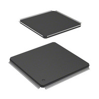
HD6417705F133BV Renesas Electronics America, HD6417705F133BV Datasheet - Page 115

HD6417705F133BV
Manufacturer Part Number
HD6417705F133BV
Description
MPU 3V 0K PB-FREE 208 FP
Manufacturer
Renesas Electronics America
Series
SuperH® SH7700r
Datasheet
1.HD6417705F133BV.pdf
(741 pages)
Specifications of HD6417705F133BV
Core Processor
SH-3
Core Size
32-Bit
Speed
133MHz
Connectivity
EBI/EMI, FIFO, IrDA, SCI, USB
Peripherals
DMA, POR, PWM, WDT
Number Of I /o
105
Program Memory Type
ROMless
Ram Size
32K x 8
Voltage - Supply (vcc/vdd)
1.4 V ~ 1.6 V
Data Converters
A/D 4x10b
Oscillator Type
Internal
Operating Temperature
-20°C ~ 75°C
Package / Case
208-LQFP
Lead Free Status / RoHS Status
Lead free / RoHS Compliant
Eeprom Size
-
Program Memory Size
-
- Current page: 115 of 741
- Download datasheet (5Mb)
3.1.1
Virtual Address Space: This LSI supports a 32-bit virtual address space that enables access to a
4-Gbyte address space. As shown in figures 3.2 and 3.3, the virtual address space is divided into
several areas. In privileged mode, a 4-Gbyte space comprising areas P0 to P4 is accessible. In user
mode, a 2-Gbyte space of U0 area is accessible. Access to any area excluding the U0 area in user
mode will result in an address error.
If the MMU is enabled by setting the AT bit of the MMUCR register to 1, P0, P3, and U0 areas
can be used as any physical address area in 1- or 4-kbyte page units. By using an 8-bit address
space identifier, P0, P2, and U0 areas can be increased to up to 256 areas. Mapping from virtual
address to 29-bit physical address can be achieved by the TLB.
1. P0, P3, and U0 Areas
2. P1 Area
3. P2 Area
4. P4 Area
The P0, P3, and U0 areas can be address translated by the TLB and can be accessed through
the cache. If the MMU is enabled, these areas can be mapped to any physical address space in
1- or 4-kbyte page units via the TLB. If the CE bit in the cache control register (CCR1) is set
to 1 and if the corresponding cache enable bit (C bit) of the TLB entry is set to 1, access via the
cache is enabled. If the MMU is disabled, replacing the upper three bits of an address in these
areas with 0s creates the address in the corresponding physical address space. If the CE bit of
the CCR1 register is set to 1, access via the cache is enabled. When the cache is used, either
the copy-back or write-through mode is selected for write access via the WT bit in CCR1.
If these areas are mapped to the on-chip module control register area in area 1 in the physical
address space via the TLB, the C bit of the corresponding page must be cleared to 0.
The P1 area can be accessed via the cache and cannot be address-translated by the TLB.
Whether the MMU is enabled or not, replacing the upper three bits of an address in these areas
with 0s creates the address in the corresponding physical address space. Use of the cache is
determined by the CE bit in the cache control register (CCR1). When the cache is used, either
the copy-back or write-through mode is selected for write access by the CB bit in the CCR1
register.
The P2 area cannot be accessed via the cache and cannot be address-translated by the TLB.
Whether the MMU is enabled or not, replacing the upper three bits of an address in this area
with 0s creates the address in the corresponding physical address space.
The P4 area is mapped to the on-chip module control register of this LSI. This area cannot be
accessed via the cache and cannot be address-translated by the TLB. Figure 3.4 shows the
configuration of the P4 area.
MMU of This LSI
Rev. 2.00, 09/03, page 67 of 690
Related parts for HD6417705F133BV
Image
Part Number
Description
Manufacturer
Datasheet
Request
R

Part Number:
Description:
KIT STARTER FOR M16C/29
Manufacturer:
Renesas Electronics America
Datasheet:

Part Number:
Description:
KIT STARTER FOR R8C/2D
Manufacturer:
Renesas Electronics America
Datasheet:

Part Number:
Description:
R0K33062P STARTER KIT
Manufacturer:
Renesas Electronics America
Datasheet:

Part Number:
Description:
KIT STARTER FOR R8C/23 E8A
Manufacturer:
Renesas Electronics America
Datasheet:

Part Number:
Description:
KIT STARTER FOR R8C/25
Manufacturer:
Renesas Electronics America
Datasheet:

Part Number:
Description:
KIT STARTER H8S2456 SHARPE DSPLY
Manufacturer:
Renesas Electronics America
Datasheet:

Part Number:
Description:
KIT STARTER FOR R8C38C
Manufacturer:
Renesas Electronics America
Datasheet:

Part Number:
Description:
KIT STARTER FOR R8C35C
Manufacturer:
Renesas Electronics America
Datasheet:

Part Number:
Description:
KIT STARTER FOR R8CL3AC+LCD APPS
Manufacturer:
Renesas Electronics America
Datasheet:

Part Number:
Description:
KIT STARTER FOR RX610
Manufacturer:
Renesas Electronics America
Datasheet:

Part Number:
Description:
KIT STARTER FOR R32C/118
Manufacturer:
Renesas Electronics America
Datasheet:

Part Number:
Description:
KIT DEV RSK-R8C/26-29
Manufacturer:
Renesas Electronics America
Datasheet:

Part Number:
Description:
KIT STARTER FOR SH7124
Manufacturer:
Renesas Electronics America
Datasheet:

Part Number:
Description:
KIT STARTER FOR H8SX/1622
Manufacturer:
Renesas Electronics America
Datasheet:

Part Number:
Description:
KIT DEV FOR SH7203
Manufacturer:
Renesas Electronics America
Datasheet:


