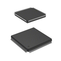
HD6417750RF200DV Renesas Electronics America, HD6417750RF200DV Datasheet - Page 170

HD6417750RF200DV
Manufacturer Part Number
HD6417750RF200DV
Description
MPU 1.5/3.3V 0K I-TEMP PB-FREE 2
Manufacturer
Renesas Electronics America
Series
SuperH® SH7750r
Datasheet
1.D6417750RBP240DV.pdf
(1164 pages)
Specifications of HD6417750RF200DV
Core Processor
SH-4
Core Size
32-Bit
Speed
200MHz
Connectivity
EBI/EMI, FIFO, SCI, SmartCard
Peripherals
DMA, POR, WDT
Number Of I /o
28
Program Memory Type
ROMless
Ram Size
48K x 8
Voltage - Supply (vcc/vdd)
1.35 V ~ 1.6 V
Oscillator Type
External
Operating Temperature
-40°C ~ 85°C
Package / Case
208-QFP Exposed Pad, 208-eQFP, 208-HQFP
Lead Free Status / RoHS Status
Lead free / RoHS Compliant
Eeprom Size
-
Program Memory Size
-
Data Converters
-
Available stocks
Company
Part Number
Manufacturer
Quantity
Price
Company:
Part Number:
HD6417750RF200DV
Manufacturer:
FREESCALE
Quantity:
450
- Current page: 170 of 1164
- Download datasheet (7Mb)
Section 3 Memory Management Unit (MMU)
0 for the C bit on that page. At that time, the regions are accessed by the values of SA and TC set
in page units of the TLB.
Here, access to the PCMCIA interface area by accessing an area of P1, P2, or P4 from the CPU is
disabled.
In addition, the PCMCIA interface area is always accessed by the DMAC with the values of
CHCRn.SSAn, CHCRn.DSAn, CHCRn.STC, and CHCRn.DTC in the DMAC. For details, see
section 14, Direct Memory Access Controller (DMAC).
P0, P3, U0 Areas: The P0 area (excluding addresses H'7C00 0000 to H'7FFF FFFF), P3 area, and
U0 area (excluding addresses H'7C00 0000 to H'7FFF FFFF) allow access using the cache and
address translation using the TLB. These areas can be mapped onto any external memory space in
1-, 4-, or 64-Kbyte, or 1-Mbyte, page units. When CCR is in the cache-enabled state and the TLB
enable bit (C bit) is 1, accesses can be performed using the cache. In write accesses to the cache,
switching between the copy-back method and the write-through method is indicated by the TLB
write-through bit (WT bit), and is specified in page units.
Only when the P0, P3, and U0 areas are mapped onto external memory space by means of the
TLB, addresses H'1C00 0000 to H'1FFF FFFF of area 7 in external memory space are allocated to
the control register area. This enables on-chip peripheral module control registers to be accessed
from the U0 area in user mode. In this case, the C bit for the corresponding page must be cleared
to 0.
P1, P2, P4 Areas: Address translation using the TLB cannot be performed for the P1, P2, or P4
area (except for the store queue area). Accesses to these areas are the same as for physical memory
space. The store queue area can be mapped onto any external memory space by the MMU.
However, operation in the case of an exception differs from that for normal P0, U0, and P3 spaces.
For details, see section 4.7, Store Queues.
3.3.4
On-Chip RAM Space
In the SH-4, half of the instruction cache can be used as on-chip RAM. This can be done by
changing the CCR settings.
When the operand cache is used as on-chip RAM (CCR.ORA = 1), P0 area addresses H'7C00
0000 to H'7FFF FFFF are an on-chip RAM area. Data accesses (byte/word/longword/quadword)
can be used in this area. This area can only be used in RAM mode.
Rev.7.00 Oct. 10, 2008 Page 84 of 1074
REJ09B0366-0700
Related parts for HD6417750RF200DV
Image
Part Number
Description
Manufacturer
Datasheet
Request
R

Part Number:
Description:
KIT STARTER FOR M16C/29
Manufacturer:
Renesas Electronics America
Datasheet:

Part Number:
Description:
KIT STARTER FOR R8C/2D
Manufacturer:
Renesas Electronics America
Datasheet:

Part Number:
Description:
R0K33062P STARTER KIT
Manufacturer:
Renesas Electronics America
Datasheet:

Part Number:
Description:
KIT STARTER FOR R8C/23 E8A
Manufacturer:
Renesas Electronics America
Datasheet:

Part Number:
Description:
KIT STARTER FOR R8C/25
Manufacturer:
Renesas Electronics America
Datasheet:

Part Number:
Description:
KIT STARTER H8S2456 SHARPE DSPLY
Manufacturer:
Renesas Electronics America
Datasheet:

Part Number:
Description:
KIT STARTER FOR R8C38C
Manufacturer:
Renesas Electronics America
Datasheet:

Part Number:
Description:
KIT STARTER FOR R8C35C
Manufacturer:
Renesas Electronics America
Datasheet:

Part Number:
Description:
KIT STARTER FOR R8CL3AC+LCD APPS
Manufacturer:
Renesas Electronics America
Datasheet:

Part Number:
Description:
KIT STARTER FOR RX610
Manufacturer:
Renesas Electronics America
Datasheet:

Part Number:
Description:
KIT STARTER FOR R32C/118
Manufacturer:
Renesas Electronics America
Datasheet:

Part Number:
Description:
KIT DEV RSK-R8C/26-29
Manufacturer:
Renesas Electronics America
Datasheet:

Part Number:
Description:
KIT STARTER FOR SH7124
Manufacturer:
Renesas Electronics America
Datasheet:

Part Number:
Description:
KIT STARTER FOR H8SX/1622
Manufacturer:
Renesas Electronics America
Datasheet:

Part Number:
Description:
KIT DEV FOR SH7203
Manufacturer:
Renesas Electronics America
Datasheet:


