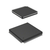
HD6417750RF200DV Renesas Electronics America, HD6417750RF200DV Datasheet - Page 857

HD6417750RF200DV
Manufacturer Part Number
HD6417750RF200DV
Description
MPU 1.5/3.3V 0K I-TEMP PB-FREE 2
Manufacturer
Renesas Electronics America
Series
SuperH® SH7750r
Datasheet
1.D6417750RBP240DV.pdf
(1164 pages)
Specifications of HD6417750RF200DV
Core Processor
SH-4
Core Size
32-Bit
Speed
200MHz
Connectivity
EBI/EMI, FIFO, SCI, SmartCard
Peripherals
DMA, POR, WDT
Number Of I /o
28
Program Memory Type
ROMless
Ram Size
48K x 8
Voltage - Supply (vcc/vdd)
1.35 V ~ 1.6 V
Oscillator Type
External
Operating Temperature
-40°C ~ 85°C
Package / Case
208-QFP Exposed Pad, 208-eQFP, 208-HQFP
Lead Free Status / RoHS Status
Lead free / RoHS Compliant
Eeprom Size
-
Program Memory Size
-
Data Converters
-
Available stocks
Company
Part Number
Manufacturer
Quantity
Price
Company:
Part Number:
HD6417750RF200DV
Manufacturer:
FREESCALE
Quantity:
450
- Current page: 857 of 1164
- Download datasheet (7Mb)
Section 16 Serial Communication Interface with FIFO (SCIF)
FIFO control register (SCFCR2). After RDF is set, receive data equivalent to the trigger number
can be read from SCFRDR2, allowing efficient continuous reception.
However, if the number of data bytes in SCFRDR2 is equal to or greater than the trigger number,
the RDF flag will be set to 1 again if it is cleared to 0. RDF should therefore be cleared to 0 after
being read as 1 after all the receive data has been read.
The number of receive data bytes in SCFRDR2 can be found from the lower 8 bits of the FIFO
data count register (SCFDR2).
Break Detection and Processing: Break signals can be detected by reading the RxD2 pin directly
when a framing error (FER) is detected. In the break state the input from the RxD2 pin consists of
all 0s, so the FER flag is set and the parity error flag (PER) may also be set.
Although the SCIF stops transferring receive data to SCFRDR2 after receiving a break, the receive
operation continues.
Sending a Break Signal: The input/output condition and level of the TxD2 pin are determined by
bits SPB2IO and SPB2DT in the serial port register (SCSPTR2). This feature can be used to send
a break signal.
After the serial transmitter is initialized, the TxD2 pin function is not selected and the value of the
SPB2DT bit substitutes for the mark state until the TE bit is set to 1 (i.e. transmission is enabled).
The SPB2IO and SPB2DT bits should therefore be set to 1 (designating output and high level)
beforehand.
To send a break signal during serial transmission, clear the SPB2DT bit to 0 (designating low
level), then clear the TE bit to 0 (halting transmission). When the TE bit is cleared to 0, the
transmitter is initialized, regardless of its current state, and 0 is output from the TxD2 pin.
Receive Data Sampling Timing and Receive Margin: The SCIF operates on a base clock with a
frequency of 16 times the transfer rate. In reception, the SCIF synchronizes internally with the fall
of the start bit, which it samples on the base clock. Receive data is latched at the rising edge of the
eighth base clock pulse. The timing is shown in figure 16.13.
Rev.7.00 Oct. 10, 2008 Page 771 of 1074
REJ09B0366-0700
Related parts for HD6417750RF200DV
Image
Part Number
Description
Manufacturer
Datasheet
Request
R

Part Number:
Description:
KIT STARTER FOR M16C/29
Manufacturer:
Renesas Electronics America
Datasheet:

Part Number:
Description:
KIT STARTER FOR R8C/2D
Manufacturer:
Renesas Electronics America
Datasheet:

Part Number:
Description:
R0K33062P STARTER KIT
Manufacturer:
Renesas Electronics America
Datasheet:

Part Number:
Description:
KIT STARTER FOR R8C/23 E8A
Manufacturer:
Renesas Electronics America
Datasheet:

Part Number:
Description:
KIT STARTER FOR R8C/25
Manufacturer:
Renesas Electronics America
Datasheet:

Part Number:
Description:
KIT STARTER H8S2456 SHARPE DSPLY
Manufacturer:
Renesas Electronics America
Datasheet:

Part Number:
Description:
KIT STARTER FOR R8C38C
Manufacturer:
Renesas Electronics America
Datasheet:

Part Number:
Description:
KIT STARTER FOR R8C35C
Manufacturer:
Renesas Electronics America
Datasheet:

Part Number:
Description:
KIT STARTER FOR R8CL3AC+LCD APPS
Manufacturer:
Renesas Electronics America
Datasheet:

Part Number:
Description:
KIT STARTER FOR RX610
Manufacturer:
Renesas Electronics America
Datasheet:

Part Number:
Description:
KIT STARTER FOR R32C/118
Manufacturer:
Renesas Electronics America
Datasheet:

Part Number:
Description:
KIT DEV RSK-R8C/26-29
Manufacturer:
Renesas Electronics America
Datasheet:

Part Number:
Description:
KIT STARTER FOR SH7124
Manufacturer:
Renesas Electronics America
Datasheet:

Part Number:
Description:
KIT STARTER FOR H8SX/1622
Manufacturer:
Renesas Electronics America
Datasheet:

Part Number:
Description:
KIT DEV FOR SH7203
Manufacturer:
Renesas Electronics America
Datasheet:


