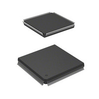
HD6417750RF200DV Renesas Electronics America, HD6417750RF200DV Datasheet - Page 579

HD6417750RF200DV
Manufacturer Part Number
HD6417750RF200DV
Description
MPU 1.5/3.3V 0K I-TEMP PB-FREE 2
Manufacturer
Renesas Electronics America
Series
SuperH® SH7750r
Datasheet
1.D6417750RBP240DV.pdf
(1164 pages)
Specifications of HD6417750RF200DV
Core Processor
SH-4
Core Size
32-Bit
Speed
200MHz
Connectivity
EBI/EMI, FIFO, SCI, SmartCard
Peripherals
DMA, POR, WDT
Number Of I /o
28
Program Memory Type
ROMless
Ram Size
48K x 8
Voltage - Supply (vcc/vdd)
1.35 V ~ 1.6 V
Oscillator Type
External
Operating Temperature
-40°C ~ 85°C
Package / Case
208-QFP Exposed Pad, 208-eQFP, 208-HQFP
Lead Free Status / RoHS Status
Lead free / RoHS Compliant
Eeprom Size
-
Program Memory Size
-
Data Converters
-
Available stocks
Company
Part Number
Manufacturer
Quantity
Price
Company:
Part Number:
HD6417750RF200DV
Manufacturer:
FREESCALE
Quantity:
450
- Current page: 579 of 1164
- Download datasheet (7Mb)
Section 13 Bus State Controller (BSC)
In a synchronous DRAM cycle, the BS signal is asserted for one cycle at the beginning of each
data transfer cycle that is in response to a READ or READA command. Data are accessed in
the following sequence: in the fill operation for a cache miss, the data between 64-bit
boundaries that include the missing data are first read by the initial READ command; after
that, the data between 16-bit boundaries data that include the missing data are read in a
wraparound way. The subsequently issued READA command reads the 16 bytes of data,
which is the remainder of the data between 32-byte boundaries, from the start of the 16-byte
boundary.
• Burst Write
Figure 13.44 is the timing chart for a burst-write operation with a burst length of 4. In this LSI,
a burst write takes place when a 32-byte data transfer has occurred. In a burst-write operation,
subsequent to the Tr cycle, in which ACTV command output takes place, a WRIT command is
issued during the Tc1 cycle, and a WRITA command is issued four cycles later. During the
write cycle, write data is output together with the write command. With a write command that
includes an auto precharge, the precharge is performed on the relevant bank of the
synchronous DRAM on completion of the write command so no new command that accesses
the same bank can be issued until precharging is completed. For this reason, in addition to the
Tpc precharge-waiting cycle used in read access, Trwl cycles, which are a period of waiting
for precharging to start after the write command, are added. These cycles delay the issuing of
new commands to the synchronous DRAM. These cycles delay the issuing of new commands
to the synchronous DRAM. The setting of the TRWL2 to TRWL0 bits of MCR selects the
number of Trwl cycles. The data between 16-byte boundaries is first accessed, and the data
between 32-byte boundaries are then written in a wraparound way.
DACK is asserted for two cycles before the data-write cycle.
Rev.7.00 Oct. 10, 2008 Page 493 of 1074
REJ09B0366-0700
Related parts for HD6417750RF200DV
Image
Part Number
Description
Manufacturer
Datasheet
Request
R

Part Number:
Description:
KIT STARTER FOR M16C/29
Manufacturer:
Renesas Electronics America
Datasheet:

Part Number:
Description:
KIT STARTER FOR R8C/2D
Manufacturer:
Renesas Electronics America
Datasheet:

Part Number:
Description:
R0K33062P STARTER KIT
Manufacturer:
Renesas Electronics America
Datasheet:

Part Number:
Description:
KIT STARTER FOR R8C/23 E8A
Manufacturer:
Renesas Electronics America
Datasheet:

Part Number:
Description:
KIT STARTER FOR R8C/25
Manufacturer:
Renesas Electronics America
Datasheet:

Part Number:
Description:
KIT STARTER H8S2456 SHARPE DSPLY
Manufacturer:
Renesas Electronics America
Datasheet:

Part Number:
Description:
KIT STARTER FOR R8C38C
Manufacturer:
Renesas Electronics America
Datasheet:

Part Number:
Description:
KIT STARTER FOR R8C35C
Manufacturer:
Renesas Electronics America
Datasheet:

Part Number:
Description:
KIT STARTER FOR R8CL3AC+LCD APPS
Manufacturer:
Renesas Electronics America
Datasheet:

Part Number:
Description:
KIT STARTER FOR RX610
Manufacturer:
Renesas Electronics America
Datasheet:

Part Number:
Description:
KIT STARTER FOR R32C/118
Manufacturer:
Renesas Electronics America
Datasheet:

Part Number:
Description:
KIT DEV RSK-R8C/26-29
Manufacturer:
Renesas Electronics America
Datasheet:

Part Number:
Description:
KIT STARTER FOR SH7124
Manufacturer:
Renesas Electronics America
Datasheet:

Part Number:
Description:
KIT STARTER FOR H8SX/1622
Manufacturer:
Renesas Electronics America
Datasheet:

Part Number:
Description:
KIT DEV FOR SH7203
Manufacturer:
Renesas Electronics America
Datasheet:


