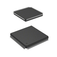
HD6417750RF200DV Renesas Electronics America, HD6417750RF200DV Datasheet - Page 555

HD6417750RF200DV
Manufacturer Part Number
HD6417750RF200DV
Description
MPU 1.5/3.3V 0K I-TEMP PB-FREE 2
Manufacturer
Renesas Electronics America
Series
SuperH® SH7750r
Datasheet
1.D6417750RBP240DV.pdf
(1164 pages)
Specifications of HD6417750RF200DV
Core Processor
SH-4
Core Size
32-Bit
Speed
200MHz
Connectivity
EBI/EMI, FIFO, SCI, SmartCard
Peripherals
DMA, POR, WDT
Number Of I /o
28
Program Memory Type
ROMless
Ram Size
48K x 8
Voltage - Supply (vcc/vdd)
1.35 V ~ 1.6 V
Oscillator Type
External
Operating Temperature
-40°C ~ 85°C
Package / Case
208-QFP Exposed Pad, 208-eQFP, 208-HQFP
Lead Free Status / RoHS Status
Lead free / RoHS Compliant
Eeprom Size
-
Program Memory Size
-
Data Converters
-
Available stocks
Company
Part Number
Manufacturer
Quantity
Price
Company:
Part Number:
HD6417750RF200DV
Manufacturer:
FREESCALE
Quantity:
450
- Current page: 555 of 1164
- Download datasheet (7Mb)
command output cycle Tc1 to the first read data latch cycle, Td1, can be specified as 1 to 5 cycles
independently for areas 2 and 3 by means of bits A2W2–A2W0 and A3W2–A3W0 in WCR2. This
number of cycles corresponds to the number of synchronous DRAM CAS latency cycles.
Note: For DACKn, an example is shown where CHCRn.AL (access level) = 0 for the DMAC.
CKIO
Bank
Precharge-sel
Address
CSn
RD/WR
RAS
CASS
DQMn
D63–D0
(read)
BS
CKE
DACKn
(SA: IO ← memory)
Figure 13.28 Basic Timing for Synchronous DRAM Burst Read
Tr
Row
Row
Row
Trw
Tc1
H/L
c0
Tc2
Tc3
Tc4/Td1
Rev.7.00 Oct. 10, 2008 Page 469 of 1074
Section 13 Bus State Controller (BSC)
d0
Td2
d1
Td3
d2
Td4
REJ09B0366-0700
d3
Related parts for HD6417750RF200DV
Image
Part Number
Description
Manufacturer
Datasheet
Request
R

Part Number:
Description:
KIT STARTER FOR M16C/29
Manufacturer:
Renesas Electronics America
Datasheet:

Part Number:
Description:
KIT STARTER FOR R8C/2D
Manufacturer:
Renesas Electronics America
Datasheet:

Part Number:
Description:
R0K33062P STARTER KIT
Manufacturer:
Renesas Electronics America
Datasheet:

Part Number:
Description:
KIT STARTER FOR R8C/23 E8A
Manufacturer:
Renesas Electronics America
Datasheet:

Part Number:
Description:
KIT STARTER FOR R8C/25
Manufacturer:
Renesas Electronics America
Datasheet:

Part Number:
Description:
KIT STARTER H8S2456 SHARPE DSPLY
Manufacturer:
Renesas Electronics America
Datasheet:

Part Number:
Description:
KIT STARTER FOR R8C38C
Manufacturer:
Renesas Electronics America
Datasheet:

Part Number:
Description:
KIT STARTER FOR R8C35C
Manufacturer:
Renesas Electronics America
Datasheet:

Part Number:
Description:
KIT STARTER FOR R8CL3AC+LCD APPS
Manufacturer:
Renesas Electronics America
Datasheet:

Part Number:
Description:
KIT STARTER FOR RX610
Manufacturer:
Renesas Electronics America
Datasheet:

Part Number:
Description:
KIT STARTER FOR R32C/118
Manufacturer:
Renesas Electronics America
Datasheet:

Part Number:
Description:
KIT DEV RSK-R8C/26-29
Manufacturer:
Renesas Electronics America
Datasheet:

Part Number:
Description:
KIT STARTER FOR SH7124
Manufacturer:
Renesas Electronics America
Datasheet:

Part Number:
Description:
KIT STARTER FOR H8SX/1622
Manufacturer:
Renesas Electronics America
Datasheet:

Part Number:
Description:
KIT DEV FOR SH7203
Manufacturer:
Renesas Electronics America
Datasheet:


