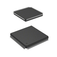
HD6417750RF200DV Renesas Electronics America, HD6417750RF200DV Datasheet - Page 587

HD6417750RF200DV
Manufacturer Part Number
HD6417750RF200DV
Description
MPU 1.5/3.3V 0K I-TEMP PB-FREE 2
Manufacturer
Renesas Electronics America
Series
SuperH® SH7750r
Datasheet
1.D6417750RBP240DV.pdf
(1164 pages)
Specifications of HD6417750RF200DV
Core Processor
SH-4
Core Size
32-Bit
Speed
200MHz
Connectivity
EBI/EMI, FIFO, SCI, SmartCard
Peripherals
DMA, POR, WDT
Number Of I /o
28
Program Memory Type
ROMless
Ram Size
48K x 8
Voltage - Supply (vcc/vdd)
1.35 V ~ 1.6 V
Oscillator Type
External
Operating Temperature
-40°C ~ 85°C
Package / Case
208-QFP Exposed Pad, 208-eQFP, 208-HQFP
Lead Free Status / RoHS Status
Lead free / RoHS Compliant
Eeprom Size
-
Program Memory Size
-
Data Converters
-
Available stocks
Company
Part Number
Manufacturer
Quantity
Price
Company:
Part Number:
HD6417750RF200DV
Manufacturer:
FREESCALE
Quantity:
450
- Current page: 587 of 1164
- Download datasheet (7Mb)
The setting for wait cycles during a bus access can also be made in MMU page units. When the
TC bit to be accessed is cleared to 0, bits A5W2 to A5W0 in wait control register 2 (WCR2), and
bits A5PCW1 and A5PCW0, A5TED2 to A5TED0, and A5TEH2 to A5TEH0 in the PCMCIA
control register (PCR), are selected. When the TC bit to be accessed is set to 1, bits A6W2 to
A6W0 in wait control register 2 (WCR2), and bits A6PCW1 and A6PCW0, A6TED2 to A6TED0,
and A6TEH2 to A6TEH0 in the PCMCIA control register (PCR), are selected. For the method of
setting bits SA2 to SA0 and bit TC for the page to be accessed, see section 3, Memory
Management Unit (MMU).
In the SH7750S and SH7750R, the PCMCIA interface can be accessed even when the MMU is
not used. When the MMU is off (MMUCR.AT=0), access is always performed by means of bits
SA2 to SA0 and bit TC in the page table entry assistance register (PTEA). When the MMU is on
(MMUCR.AT=1), the situation is the same as for the SH7750.
In this LSI, access to a PCMCIA interface area by the DMAC is always performed using the
DMAC's CHCRn.SSAn, CHCRn.DSAn, CHCRn.STC, and CHCRn.DTC values.
SA2
0
1
AnPCW1–AnPCW0 specify the number of wait states to be inserted in a low-speed bus cycle; a
value of 0, 15, 30, or 50 can be set, and this value is added to the number of wait states for
insertion specified by WCR2. AnTED2–AnTED0 can be set to a value from 0 to 15, enabling the
address, CS, CE2A, CE2B, and REG setup times with respect to the RD and WE1 signals to be
secured. AnTEH2–AnTEH0 can also be set to a value from 0 to 15, enabling the address, CS,
CE2A, CE2B, and REG write data hold times with respect to the RD and WE1 signals to be
secured.
Wait cycles between cycles are set with bits A5IW2–A5IW0 and A6IW2–A6IW0 in wait control
register 1 (WCR1). The inter-cycle write cycles selected depend only on the area accessed (area 5
or 6): when area 5 is accessed, bits A5IW2–A5IW0 are selected, and when area 6 is accessed, bits
A6IW2–A6IW0 are selected.
SA1
0
1
0
1
SA0
0
1
0
1
0
1
0
1
Description
Reserved (Setting prohibited)
Dynamic I/O bus sizing
8-bit I/O space
16-bit I/O space
8-bit common memory
16-bit common memory
8-bit attribute memory
16-bit attribute memory
Rev.7.00 Oct. 10, 2008 Page 501 of 1074
Section 13 Bus State Controller (BSC)
REJ09B0366-0700
Related parts for HD6417750RF200DV
Image
Part Number
Description
Manufacturer
Datasheet
Request
R

Part Number:
Description:
KIT STARTER FOR M16C/29
Manufacturer:
Renesas Electronics America
Datasheet:

Part Number:
Description:
KIT STARTER FOR R8C/2D
Manufacturer:
Renesas Electronics America
Datasheet:

Part Number:
Description:
R0K33062P STARTER KIT
Manufacturer:
Renesas Electronics America
Datasheet:

Part Number:
Description:
KIT STARTER FOR R8C/23 E8A
Manufacturer:
Renesas Electronics America
Datasheet:

Part Number:
Description:
KIT STARTER FOR R8C/25
Manufacturer:
Renesas Electronics America
Datasheet:

Part Number:
Description:
KIT STARTER H8S2456 SHARPE DSPLY
Manufacturer:
Renesas Electronics America
Datasheet:

Part Number:
Description:
KIT STARTER FOR R8C38C
Manufacturer:
Renesas Electronics America
Datasheet:

Part Number:
Description:
KIT STARTER FOR R8C35C
Manufacturer:
Renesas Electronics America
Datasheet:

Part Number:
Description:
KIT STARTER FOR R8CL3AC+LCD APPS
Manufacturer:
Renesas Electronics America
Datasheet:

Part Number:
Description:
KIT STARTER FOR RX610
Manufacturer:
Renesas Electronics America
Datasheet:

Part Number:
Description:
KIT STARTER FOR R32C/118
Manufacturer:
Renesas Electronics America
Datasheet:

Part Number:
Description:
KIT DEV RSK-R8C/26-29
Manufacturer:
Renesas Electronics America
Datasheet:

Part Number:
Description:
KIT STARTER FOR SH7124
Manufacturer:
Renesas Electronics America
Datasheet:

Part Number:
Description:
KIT STARTER FOR H8SX/1622
Manufacturer:
Renesas Electronics America
Datasheet:

Part Number:
Description:
KIT DEV FOR SH7203
Manufacturer:
Renesas Electronics America
Datasheet:


