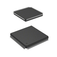
HD6417750RF200DV Renesas Electronics America, HD6417750RF200DV Datasheet - Page 201

HD6417750RF200DV
Manufacturer Part Number
HD6417750RF200DV
Description
MPU 1.5/3.3V 0K I-TEMP PB-FREE 2
Manufacturer
Renesas Electronics America
Series
SuperH® SH7750r
Datasheet
1.D6417750RBP240DV.pdf
(1164 pages)
Specifications of HD6417750RF200DV
Core Processor
SH-4
Core Size
32-Bit
Speed
200MHz
Connectivity
EBI/EMI, FIFO, SCI, SmartCard
Peripherals
DMA, POR, WDT
Number Of I /o
28
Program Memory Type
ROMless
Ram Size
48K x 8
Voltage - Supply (vcc/vdd)
1.35 V ~ 1.6 V
Oscillator Type
External
Operating Temperature
-40°C ~ 85°C
Package / Case
208-QFP Exposed Pad, 208-eQFP, 208-HQFP
Lead Free Status / RoHS Status
Lead free / RoHS Compliant
Eeprom Size
-
Program Memory Size
-
Data Converters
-
Available stocks
Company
Part Number
Manufacturer
Quantity
Price
Company:
Part Number:
HD6417750RF200DV
Manufacturer:
FREESCALE
Quantity:
450
- Current page: 201 of 1164
- Download datasheet (7Mb)
an instruction that performs data access to the P0, P1, P3, or U0 area should be located at least
four instructions after the CCR update instruction. Also, a branch instruction to the P0, P1, P3, or
U0 area should be located at least eight instructions after the CCR update instruction.
• EMODE: Double-sized cache mode bit
• IIX: IC index enable bit
• ICI: IC invalidation bit
• ICE: IC enable bit
• OIX: OC index enable bit*
• ORA: OC RAM enable bit*
• OCI: OC invalidation bit
In the SH7750R, this bit indicates whether the double-sized cache mode is used or not.
This bit is reserved in the SH7750 and SH7750S. The EMODE bit must not be written to while
the cache is being used.
0: SH7750/SH7750S-compatible mode*
1: Double-sized cache mode
0: Effective address bits [12:5] used for IC entry selection
1: Effective address bits [25] and [11:5] used for IC entry selection
When 1 is written to this bit, the V bits of all IC entries are cleared to 0. This bit always returns
0 when read.
Indicates whether or not the IC is to be used. When address translation is performed, the IC
cannot be used unless the C bit in the page management information is also 1.
0: IC not used
1: IC used
0: Effective address bits [13:5] used for OC entry selection
1: Effective address bits [25] and [12:5] used for OC entry selection
When the OC is enabled (OCE = 1), the ORA bit specifies whether the half of the OC are to be
used as RAM. When the OC is not enabled (OCE = 0), the ORA bit should be cleared to 0.
0: Normal mode (the entire OC is used as a cache)
1: RAM mode (half of the OC is used as a cache and the other half is used as RAM)
When 1 is written to this bit, the V and U bits of all OC entries are cleared to 0. This bit always
returns 0 when read.
2
3
1
(initial value)
Rev.7.00 Oct. 10, 2008 Page 115 of 1074
REJ09B0366-0700
Section 4 Caches
Related parts for HD6417750RF200DV
Image
Part Number
Description
Manufacturer
Datasheet
Request
R

Part Number:
Description:
KIT STARTER FOR M16C/29
Manufacturer:
Renesas Electronics America
Datasheet:

Part Number:
Description:
KIT STARTER FOR R8C/2D
Manufacturer:
Renesas Electronics America
Datasheet:

Part Number:
Description:
R0K33062P STARTER KIT
Manufacturer:
Renesas Electronics America
Datasheet:

Part Number:
Description:
KIT STARTER FOR R8C/23 E8A
Manufacturer:
Renesas Electronics America
Datasheet:

Part Number:
Description:
KIT STARTER FOR R8C/25
Manufacturer:
Renesas Electronics America
Datasheet:

Part Number:
Description:
KIT STARTER H8S2456 SHARPE DSPLY
Manufacturer:
Renesas Electronics America
Datasheet:

Part Number:
Description:
KIT STARTER FOR R8C38C
Manufacturer:
Renesas Electronics America
Datasheet:

Part Number:
Description:
KIT STARTER FOR R8C35C
Manufacturer:
Renesas Electronics America
Datasheet:

Part Number:
Description:
KIT STARTER FOR R8CL3AC+LCD APPS
Manufacturer:
Renesas Electronics America
Datasheet:

Part Number:
Description:
KIT STARTER FOR RX610
Manufacturer:
Renesas Electronics America
Datasheet:

Part Number:
Description:
KIT STARTER FOR R32C/118
Manufacturer:
Renesas Electronics America
Datasheet:

Part Number:
Description:
KIT DEV RSK-R8C/26-29
Manufacturer:
Renesas Electronics America
Datasheet:

Part Number:
Description:
KIT STARTER FOR SH7124
Manufacturer:
Renesas Electronics America
Datasheet:

Part Number:
Description:
KIT STARTER FOR H8SX/1622
Manufacturer:
Renesas Electronics America
Datasheet:

Part Number:
Description:
KIT DEV FOR SH7203
Manufacturer:
Renesas Electronics America
Datasheet:


