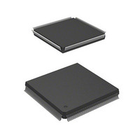
HD6417750RF200DV Renesas Electronics America, HD6417750RF200DV Datasheet - Page 876

HD6417750RF200DV
Manufacturer Part Number
HD6417750RF200DV
Description
MPU 1.5/3.3V 0K I-TEMP PB-FREE 2
Manufacturer
Renesas Electronics America
Series
SuperH® SH7750r
Datasheet
1.D6417750RBP240DV.pdf
(1164 pages)
Specifications of HD6417750RF200DV
Core Processor
SH-4
Core Size
32-Bit
Speed
200MHz
Connectivity
EBI/EMI, FIFO, SCI, SmartCard
Peripherals
DMA, POR, WDT
Number Of I /o
28
Program Memory Type
ROMless
Ram Size
48K x 8
Voltage - Supply (vcc/vdd)
1.35 V ~ 1.6 V
Oscillator Type
External
Operating Temperature
-40°C ~ 85°C
Package / Case
208-QFP Exposed Pad, 208-eQFP, 208-HQFP
Lead Free Status / RoHS Status
Lead free / RoHS Compliant
Eeprom Size
-
Program Memory Size
-
Data Converters
-
Available stocks
Company
Part Number
Manufacturer
Quantity
Price
Company:
Part Number:
HD6417750RF200DV
Manufacturer:
FREESCALE
Quantity:
450
- Current page: 876 of 1164
- Download datasheet (7Mb)
Section 17 Smart Card Interface
17.3.6
Initialization: Before transmitting and receiving data, the smart card interface must be initialized
as described below. Initialization is also necessary when switching from transmit mode to receive
mode, or vice versa. Figure 17.7 shows a sample initialization processing flowchart.
1. Clear the TE and RE bits in the serial control register (SCSCR1) to 0.
2. Clear error flags FER/ERS, PER, and ORER in the serial status register (SCSSR1) to 0.
3. Set the GM bit, parity bit (O/E), and baud rate generator select bits (CKS1 and CKS0) in the
4. Set the SMIF, SDIR, and SINV bits in the smart card mode register (SCSCMR1).
5. Set the value corresponding to the bit rate in the bit rate register (SCBRR1).
6. Set the clock source select bits (CKE1 and CKE0) in SCSCR1. Clear the TIE, RIE, TE, RE,
7. Wait at least one bit interval, then set the TIE, RIE, TE, and RE bits in SCSCR1. Do not set the
Rev.7.00 Oct. 10, 2008 Page 790 of 1074
REJ09B0366-0700
CKE1 value
Port value
SCK
SCK
serial mode register (SCSMR1). Clear the CHR and MP bits to 0, and set the STOP and PE
bits to 1.
When the SMIF bit is set to 1, the TxD pin and RxD pin both go to the high-impedance state.
MPIE, and TEIE bits to 0.
If the CKE0 bit is set to 1, the clock is output from the SCK pin.
TE bit and RE bit at the same time, except for self-diagnosis.
Data Transmit/Receive Operations
Figure 17.6 Difference in Clock Output According to GM Bit Setting
Specified
width
Width is
undefined
(b) When GM = 1
(a) When GM = 0
Specified
width
Width is
undefined
CKE1 value
Port value
Related parts for HD6417750RF200DV
Image
Part Number
Description
Manufacturer
Datasheet
Request
R

Part Number:
Description:
KIT STARTER FOR M16C/29
Manufacturer:
Renesas Electronics America
Datasheet:

Part Number:
Description:
KIT STARTER FOR R8C/2D
Manufacturer:
Renesas Electronics America
Datasheet:

Part Number:
Description:
R0K33062P STARTER KIT
Manufacturer:
Renesas Electronics America
Datasheet:

Part Number:
Description:
KIT STARTER FOR R8C/23 E8A
Manufacturer:
Renesas Electronics America
Datasheet:

Part Number:
Description:
KIT STARTER FOR R8C/25
Manufacturer:
Renesas Electronics America
Datasheet:

Part Number:
Description:
KIT STARTER H8S2456 SHARPE DSPLY
Manufacturer:
Renesas Electronics America
Datasheet:

Part Number:
Description:
KIT STARTER FOR R8C38C
Manufacturer:
Renesas Electronics America
Datasheet:

Part Number:
Description:
KIT STARTER FOR R8C35C
Manufacturer:
Renesas Electronics America
Datasheet:

Part Number:
Description:
KIT STARTER FOR R8CL3AC+LCD APPS
Manufacturer:
Renesas Electronics America
Datasheet:

Part Number:
Description:
KIT STARTER FOR RX610
Manufacturer:
Renesas Electronics America
Datasheet:

Part Number:
Description:
KIT STARTER FOR R32C/118
Manufacturer:
Renesas Electronics America
Datasheet:

Part Number:
Description:
KIT DEV RSK-R8C/26-29
Manufacturer:
Renesas Electronics America
Datasheet:

Part Number:
Description:
KIT STARTER FOR SH7124
Manufacturer:
Renesas Electronics America
Datasheet:

Part Number:
Description:
KIT STARTER FOR H8SX/1622
Manufacturer:
Renesas Electronics America
Datasheet:

Part Number:
Description:
KIT DEV FOR SH7203
Manufacturer:
Renesas Electronics America
Datasheet:


