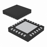
ATA8742-PXQW Atmel, ATA8742-PXQW Datasheet - Page 134

ATA8742-PXQW
Manufacturer Part Number
ATA8742-PXQW
Description
MCU W/TRANSMITTER ASK/FSK 24QFN
Manufacturer
Atmel
Datasheet
1.ATA8742-PXQW.pdf
(238 pages)
Specifications of ATA8742-PXQW
Frequency
433MHz
Applications
Home Automation, Remote Sensing, RKE
Modulation Or Protocol
ASK, FSK
Data Rate - Maximum
32 kBit/s
Power - Output
7.5dBm
Current - Transmitting
9.8mA
Data Interface
PCB, Surface Mount
Antenna Connector
PCB, Surface Mount
Memory Size
4kB Flash, 256B EEPROM, 256B SRAM
Voltage - Supply
2 V ~ 4 V
Operating Temperature
-40°C ~ 85°C
Package / Case
24-VQFN Exposed Pad, 24-HVQFN, 24-SQFN, 24-DHVQFN
Processor Series
ATA8x
Core
AVR8
Data Bus Width
8 bit
Program Memory Type
Flash
Program Memory Size
4 KB
Data Ram Size
256 B
Interface Type
SPI, USI
Maximum Clock Frequency
8.1 MHz
Number Of Programmable I/os
12
Number Of Timers
2
Maximum Operating Temperature
+ 85 C
Mounting Style
SMD/SMT
Development Tools By Supplier
ATASTK512-EK1-IND
Minimum Operating Temperature
- 40 C
On-chip Adc
10 bit, 8 Channel
Lead Free Status / RoHS Status
Lead free / RoHS Compliant
Features
-
Lead Free Status / Rohs Status
Details
Available stocks
Company
Part Number
Manufacturer
Quantity
Price
Company:
Part Number:
ATA8742-PXQW
Manufacturer:
ATMEL
Quantity:
1 482
- Current page: 134 of 238
- Download datasheet (4Mb)
21.11.7
21.11.8
134
ATA8742
ICR1H and ICR1L – Input Capture Register 1
TIMSK1 – Timer/Counter Interrupt Mask Register 1
The Input Capture is updated with the counter (TCNT1) value each time an event occurs on the
ICP1 pin (or optionally on the Analog Comparator output for Timer/Counter1). The Input Capture
can be used for defining the counter TOP value.
The Input Capture Register is 16-bit in size. To ensure that both the high and low bytes are read
simultaneously when the CPU accesses these registers, the access is performed using an 8-bit
temporary high byte register (TEMP). This temporary register is shared by all the other 16-bit
registers.
• Bit 7,6,4,3 – Reserved Bit
This bit is reserved for future use. For ensuring compatibility with future devices, this bit must be
written to zero when the register is written.
• Bit 5 – ICIE1: Timer/Counter1, Input Capture Interrupt Enable
When this bit is written to one, and the I-flag in the Status Register is set (interrupts globally
enabled), the Timer/Countern Input Capture interrupt is enabled. The
corresponding Interrupt Vector (See “Interrupts” on page 66.) is executed when the
ICF1 Flag, located in TIFR1, is set.
• Bit 2– OCIE1B: Timer/Counter1, Output Compare B Match Interrupt Enable
When this bit is written to one, and the I-flag in the Status Register is set (interrupts globally
enabled), the Timer/Counter1 Output Compare B Match interrupt is enabled. The corresponding
Interrupt Vector (see
TIFR1, is set.
• Bit 1– OCIE1A: Timer/Counter1, Output Compare A Match Interrupt Enable
When this bit is written to one, and the I-flag in the Status Register is set (interrupts globally
enabled), the Timer/Counter1 Output Compare A Match interrupt is enabled. The corresponding
Interrupt Vector (see
TIFR1, is set.
• Bit 0 – TOIE1: Timer/Counter1, Overflow Interrupt Enable
When this bit is written to one, and the I-flag in the Status Register is set (interrupts globally
enabled), the Timer/Counter1 Overflow interrupt is enabled. The corresponding Interrupt Vector
(see
Bit
0x25 (0x45)
0x24 (0x44)
Read/Write
Initial Value
Bit
0x0C (0x2C)
Read/Write
Initial Value
“Interrupts” on page
“Accessing 16-bit Registers” on page
R/W
R
7
0
7
–
0
“Interrupts” on page
“Interrupts” on page
R/W
66) is executed when the TOV1 flag, located in TIFR1, is set.
6
0
R
6
–
0
R/W
ICIE1
R/W
5
0
5
0
R/W
66) is executed when the OCF1B flag, located in
66) is executed when the OCF1A flag, located in
4
0
R
4
–
0
ICR1[15:8]
ICR1[7:0]
110.
R/W
3
0
R
3
–
0
OCIE1B
R/W
R/W
2
0
2
0
OCIE1A
R/W
R/W
1
0
1
0
R/W
TOIE1
9151A–INDCO–07/09
R/W
0
0
0
0
TIMSK1
ICR1H
ICR1L
Related parts for ATA8742-PXQW
Image
Part Number
Description
Manufacturer
Datasheet
Request
R

Part Number:
Description:
Manufacturer:
ATMEL Corporation
Datasheet:

Part Number:
Description:
DEV KIT FOR AVR/AVR32
Manufacturer:
Atmel
Datasheet:

Part Number:
Description:
INTERVAL AND WIPE/WASH WIPER CONTROL IC WITH DELAY
Manufacturer:
ATMEL Corporation
Datasheet:

Part Number:
Description:
Low-Voltage Voice-Switched IC for Hands-Free Operation
Manufacturer:
ATMEL Corporation
Datasheet:

Part Number:
Description:
MONOLITHIC INTEGRATED FEATUREPHONE CIRCUIT
Manufacturer:
ATMEL Corporation
Datasheet:

Part Number:
Description:
AM-FM Receiver IC U4255BM-M
Manufacturer:
ATMEL Corporation
Datasheet:

Part Number:
Description:
Monolithic Integrated Feature Phone Circuit
Manufacturer:
ATMEL Corporation
Datasheet:

Part Number:
Description:
Multistandard Video-IF and Quasi Parallel Sound Processing
Manufacturer:
ATMEL Corporation
Datasheet:

Part Number:
Description:
High-performance EE PLD
Manufacturer:
ATMEL Corporation
Datasheet:

Part Number:
Description:
8-bit Flash Microcontroller
Manufacturer:
ATMEL Corporation
Datasheet:

Part Number:
Description:
2-Wire Serial EEPROM
Manufacturer:
ATMEL Corporation
Datasheet:


