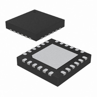
ATA8742-PXQW Atmel, ATA8742-PXQW Datasheet - Page 185

ATA8742-PXQW
Manufacturer Part Number
ATA8742-PXQW
Description
MCU W/TRANSMITTER ASK/FSK 24QFN
Manufacturer
Atmel
Datasheet
1.ATA8742-PXQW.pdf
(238 pages)
Specifications of ATA8742-PXQW
Frequency
433MHz
Applications
Home Automation, Remote Sensing, RKE
Modulation Or Protocol
ASK, FSK
Data Rate - Maximum
32 kBit/s
Power - Output
7.5dBm
Current - Transmitting
9.8mA
Data Interface
PCB, Surface Mount
Antenna Connector
PCB, Surface Mount
Memory Size
4kB Flash, 256B EEPROM, 256B SRAM
Voltage - Supply
2 V ~ 4 V
Operating Temperature
-40°C ~ 85°C
Package / Case
24-VQFN Exposed Pad, 24-HVQFN, 24-SQFN, 24-DHVQFN
Processor Series
ATA8x
Core
AVR8
Data Bus Width
8 bit
Program Memory Type
Flash
Program Memory Size
4 KB
Data Ram Size
256 B
Interface Type
SPI, USI
Maximum Clock Frequency
8.1 MHz
Number Of Programmable I/os
12
Number Of Timers
2
Maximum Operating Temperature
+ 85 C
Mounting Style
SMD/SMT
Development Tools By Supplier
ATASTK512-EK1-IND
Minimum Operating Temperature
- 40 C
On-chip Adc
10 bit, 8 Channel
Lead Free Status / RoHS Status
Lead free / RoHS Compliant
Features
-
Lead Free Status / Rohs Status
Details
Available stocks
Company
Part Number
Manufacturer
Quantity
Price
Company:
Part Number:
ATA8742-PXQW
Manufacturer:
ATMEL
Quantity:
1 482
- Current page: 185 of 238
- Download datasheet (4Mb)
28.6.1
9151A–INDCO–07/09
Serial Programming Algorithm
When writing serial data to the ATtiny24/44/84, data is clocked on the rising edge of SCK.
When reading data from the ATtiny24/44/84, data is clocked on the falling edge of SCK. See
Figure 29-3
To program and verify the ATtiny24/44/84 in the Serial Programming mode, the following
sequence is recommended (see four byte instruction formats in
1. Power-up sequence:
2. Wait for at least 20 ms and enable serial programming by sending the Programming
3. The serial programming instructions will not work if the communication is out of synchro-
4. The Flash is programmed one page at a time. The memory page is loaded one byte at a
5. A: The EEPROM array is programmed one byte at a time by supplying the address and
6. Any memory location can be verified by using the Read instruction which returns the con-
7. At the end of the programming session, RESET can be set high to commence normal
8. Power-off sequence (if needed):
Apply power between V
tems, the programmer can not guarantee that SCK is held low during power-up. In this
case, RESET must be given a positive pulse of at least two CPU clock cycles duration
after SCK has been set to “0”.
Enable serial instruction to pin MOSI.
nization. When in sync. the second byte (0x53), will echo back when issuing the third
byte of the Programming Enable instruction. Whether the echo is correct or not, all four
bytes of the instruction must be transmitted. If the 0x53 did not echo back, give RESET a
positive pulse and issue a new Programming Enable command.
time by supplying the 5 LSB of the address and data together with the Load Program
memory Page instruction. To ensure correct loading of the page, the data low byte must
be loaded before data high byte is applied for a given address. The Program memory
Page is stored by loading the Write Program memory Page instruction with the 3 MSB of
the address. If polling (RDY/BSY) is not used, the user must wait at least t
issuing the next page. (See
ming interface before the Flash write operation completes can result in incorrect
programming.
data together with the appropriate Write instruction. An EEPROM memory location is first
automatically erased before new data is written. If polling (RDY/BSY) is not used, the
user must wait at least t
page
B: The EEPROM array is programmed one page at a time. The Memory page is loaded
one byte at a time by supplying the 2 LSB of the address and data together with the Load
EEPROM Memory Page instruction. The EEPROM Memory Page is stored by loading
the Write EEPROM Memory Page Instruction with the 4 MSB of the address. When using
EEPROM page access only byte locations loaded with the Load EEPROM Memory Page
instruction is altered. The remaining locations remain unchanged. If polling (RDY/BSY) is
not used, the used must wait at least t
28-10 on page
programmed.
tent at the selected address at serial output MISO.
operation.
Set RESET to “1”.
Turn V
186.) In a chip erased device, no 0xFFs in the data file(s) need to be programmed.
CC
and
power off.
Figure 29-4
186). In a chip erased device, no 0xFF in the data file(s) need to be
CC
WD_EEPROM
for timing details.
and GND while RESET and SCK are set to “0”. In some sys-
Table 28-10 on page
before issuing the next byte. (See
WD_EEPROM
before issuing the next page (See
186.) Accessing the serial program-
Table
28-11):
Table 28-10 on
WD_FLASH
ATA8742
before
Table
185
Related parts for ATA8742-PXQW
Image
Part Number
Description
Manufacturer
Datasheet
Request
R

Part Number:
Description:
Manufacturer:
ATMEL Corporation
Datasheet:

Part Number:
Description:
DEV KIT FOR AVR/AVR32
Manufacturer:
Atmel
Datasheet:

Part Number:
Description:
INTERVAL AND WIPE/WASH WIPER CONTROL IC WITH DELAY
Manufacturer:
ATMEL Corporation
Datasheet:

Part Number:
Description:
Low-Voltage Voice-Switched IC for Hands-Free Operation
Manufacturer:
ATMEL Corporation
Datasheet:

Part Number:
Description:
MONOLITHIC INTEGRATED FEATUREPHONE CIRCUIT
Manufacturer:
ATMEL Corporation
Datasheet:

Part Number:
Description:
AM-FM Receiver IC U4255BM-M
Manufacturer:
ATMEL Corporation
Datasheet:

Part Number:
Description:
Monolithic Integrated Feature Phone Circuit
Manufacturer:
ATMEL Corporation
Datasheet:

Part Number:
Description:
Multistandard Video-IF and Quasi Parallel Sound Processing
Manufacturer:
ATMEL Corporation
Datasheet:

Part Number:
Description:
High-performance EE PLD
Manufacturer:
ATMEL Corporation
Datasheet:

Part Number:
Description:
8-bit Flash Microcontroller
Manufacturer:
ATMEL Corporation
Datasheet:

Part Number:
Description:
2-Wire Serial EEPROM
Manufacturer:
ATMEL Corporation
Datasheet:


