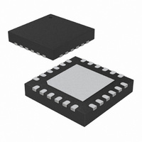
ATA8742-PXQW Atmel, ATA8742-PXQW Datasheet - Page 180

ATA8742-PXQW
Manufacturer Part Number
ATA8742-PXQW
Description
MCU W/TRANSMITTER ASK/FSK 24QFN
Manufacturer
Atmel
Datasheet
1.ATA8742-PXQW.pdf
(238 pages)
Specifications of ATA8742-PXQW
Frequency
433MHz
Applications
Home Automation, Remote Sensing, RKE
Modulation Or Protocol
ASK, FSK
Data Rate - Maximum
32 kBit/s
Power - Output
7.5dBm
Current - Transmitting
9.8mA
Data Interface
PCB, Surface Mount
Antenna Connector
PCB, Surface Mount
Memory Size
4kB Flash, 256B EEPROM, 256B SRAM
Voltage - Supply
2 V ~ 4 V
Operating Temperature
-40°C ~ 85°C
Package / Case
24-VQFN Exposed Pad, 24-HVQFN, 24-SQFN, 24-DHVQFN
Processor Series
ATA8x
Core
AVR8
Data Bus Width
8 bit
Program Memory Type
Flash
Program Memory Size
4 KB
Data Ram Size
256 B
Interface Type
SPI, USI
Maximum Clock Frequency
8.1 MHz
Number Of Programmable I/os
12
Number Of Timers
2
Maximum Operating Temperature
+ 85 C
Mounting Style
SMD/SMT
Development Tools By Supplier
ATASTK512-EK1-IND
Minimum Operating Temperature
- 40 C
On-chip Adc
10 bit, 8 Channel
Lead Free Status / RoHS Status
Lead free / RoHS Compliant
Features
-
Lead Free Status / Rohs Status
Details
Available stocks
Company
Part Number
Manufacturer
Quantity
Price
Company:
Part Number:
ATA8742-PXQW
Manufacturer:
ATMEL
Quantity:
1 482
- Current page: 180 of 238
- Download datasheet (4Mb)
28. Memory Programming
28.1
180
Program And Data Memory Lock Bits
ATA8742
This section describes the different methods for Programming the ATtiny24/44/84 memories.
The ATtiny24/44/84 provides two Lock bits which can be left unprogrammed (“1”) or can be pro-
grammed (“0”) to obtain the additional security listed in
can only be erased to “1” with the Chip Erase command.
Program memory can be read out via the debugWIRE interface when the DWEN fuse is pro-
grammed, even if the Lock Bits are set. Thus, when Lock Bit security is required, should always
debugWIRE be disabled by clearing the DWEN fuse.
Table 28-1.
Note:
Table 28-2.
Notes:
LB2
LB1
LB Mode
Lock Bit Byte
1
2
3
1. “1” means unprogrammed, “0” means programmed
1. Program the Fuse bits before programming the LB1 and LB2.
2. “1” means unprogrammed, “0” means programmed
Memory Lock Bits
Lock Bit Byte
Lock Bit Protection Modes
LB2
1
1
0
(1)
LB1
1
0
0
Bit No
7
6
5
4
3
2
1
0
Protection Type
No memory lock features enabled.
Further programming of the Flash and EEPROM is disabled in
High-voltage and Serial Programming mode. The Fuse bits are
locked in both Serial and High-voltage Programming mode.
debugWire is disabled.
Further programming and verification of the Flash and EEPROM
is disabled in High-voltage and Serial Programming mode. The
Fuse bits are locked in both Serial and High-voltage
Programming mode.
(1)(2)
Description
–
–
–
–
–
–
Lock bit
Lock bit
(1)
Table 28-2 on page
debugWire is disabled.
Default Value
1 (unprogrammed)
1 (unprogrammed)
1 (unprogrammed)
1 (unprogrammed)
1 (unprogrammed)
1 (unprogrammed)
1 (unprogrammed)
1 (unprogrammed)
180. The Lock bits
9151A–INDCO–07/09
(1)
Related parts for ATA8742-PXQW
Image
Part Number
Description
Manufacturer
Datasheet
Request
R

Part Number:
Description:
Manufacturer:
ATMEL Corporation
Datasheet:

Part Number:
Description:
DEV KIT FOR AVR/AVR32
Manufacturer:
Atmel
Datasheet:

Part Number:
Description:
INTERVAL AND WIPE/WASH WIPER CONTROL IC WITH DELAY
Manufacturer:
ATMEL Corporation
Datasheet:

Part Number:
Description:
Low-Voltage Voice-Switched IC for Hands-Free Operation
Manufacturer:
ATMEL Corporation
Datasheet:

Part Number:
Description:
MONOLITHIC INTEGRATED FEATUREPHONE CIRCUIT
Manufacturer:
ATMEL Corporation
Datasheet:

Part Number:
Description:
AM-FM Receiver IC U4255BM-M
Manufacturer:
ATMEL Corporation
Datasheet:

Part Number:
Description:
Monolithic Integrated Feature Phone Circuit
Manufacturer:
ATMEL Corporation
Datasheet:

Part Number:
Description:
Multistandard Video-IF and Quasi Parallel Sound Processing
Manufacturer:
ATMEL Corporation
Datasheet:

Part Number:
Description:
High-performance EE PLD
Manufacturer:
ATMEL Corporation
Datasheet:

Part Number:
Description:
8-bit Flash Microcontroller
Manufacturer:
ATMEL Corporation
Datasheet:

Part Number:
Description:
2-Wire Serial EEPROM
Manufacturer:
ATMEL Corporation
Datasheet:


