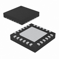
ATA8742-PXQW Atmel, ATA8742-PXQW Datasheet - Page 28

ATA8742-PXQW
Manufacturer Part Number
ATA8742-PXQW
Description
MCU W/TRANSMITTER ASK/FSK 24QFN
Manufacturer
Atmel
Datasheet
1.ATA8742-PXQW.pdf
(238 pages)
Specifications of ATA8742-PXQW
Frequency
433MHz
Applications
Home Automation, Remote Sensing, RKE
Modulation Or Protocol
ASK, FSK
Data Rate - Maximum
32 kBit/s
Power - Output
7.5dBm
Current - Transmitting
9.8mA
Data Interface
PCB, Surface Mount
Antenna Connector
PCB, Surface Mount
Memory Size
4kB Flash, 256B EEPROM, 256B SRAM
Voltage - Supply
2 V ~ 4 V
Operating Temperature
-40°C ~ 85°C
Package / Case
24-VQFN Exposed Pad, 24-HVQFN, 24-SQFN, 24-DHVQFN
Processor Series
ATA8x
Core
AVR8
Data Bus Width
8 bit
Program Memory Type
Flash
Program Memory Size
4 KB
Data Ram Size
256 B
Interface Type
SPI, USI
Maximum Clock Frequency
8.1 MHz
Number Of Programmable I/os
12
Number Of Timers
2
Maximum Operating Temperature
+ 85 C
Mounting Style
SMD/SMT
Development Tools By Supplier
ATASTK512-EK1-IND
Minimum Operating Temperature
- 40 C
On-chip Adc
10 bit, 8 Channel
Lead Free Status / RoHS Status
Lead free / RoHS Compliant
Features
-
Lead Free Status / Rohs Status
Details
Available stocks
Company
Part Number
Manufacturer
Quantity
Price
Company:
Part Number:
ATA8742-PXQW
Manufacturer:
ATMEL
Quantity:
1 482
- Current page: 28 of 238
- Download datasheet (4Mb)
12.7
12.8
28
Instruction Execution Timing
Reset and Interrupt Handling
ATA8742
This section describes the general access timing concepts for instruction execution. The AVR
CPU is driven by the CPU clock clk
chip. No internal clock division is used.
Figure 12-4 on page 28
enabled by the Harvard architecture and the fast access Register File concept. This is the basic
pipelining concept to obtain up to 1 MIPS per MHz with the corresponding unique results for
functions per cost, functions per clocks, and functions per power-unit.
Figure 12-4. The Parallel Instruction Fetches and Instruction Executions
Figure 12-5 on page 28
cycle an ALU operation using two register operands is executed, and the result is stored back to
the destination register.
Figure 12-5. Single Cycle ALU Operation
The AVR provides several different interrupt sources. These interrupts and the separate Reset
Vector each have a separate Program Vector in the Program memory space. All interrupts are
assigned individual enable bits which must be written logic one together with the Global Interrupt
Enable bit in the Status Register in order to enable the interrupt.
The lowest addresses in the Program memory space are by default defined as the Reset and
Interrupt Vectors. The complete list of vectors is shown in
determines the priority levels of the different interrupts. The lower the address the higher is the
priority level. RESET has the highest priority, and next is INT0 – the External Interrupt Request
0.
Register Operands Fetch
2nd Instruction Execute
3rd Instruction Execute
1st Instruction Execute
ALU Operation Execute
2nd Instruction Fetch
3rd Instruction Fetch
4th Instruction Fetch
1st Instruction Fetch
Total Execution Time
Result Write Back
clk
clk
CPU
CPU
shows the internal timing concept for the Register File. In a single clock
shows the parallel instruction fetches and instruction executions
CPU
T1
T1
, directly generated from the selected clock source for the
T2
T2
“Interrupts” on page
T3
T3
66. The list also
9151A–INDCO–07/09
T4
T4
Related parts for ATA8742-PXQW
Image
Part Number
Description
Manufacturer
Datasheet
Request
R

Part Number:
Description:
Manufacturer:
ATMEL Corporation
Datasheet:

Part Number:
Description:
DEV KIT FOR AVR/AVR32
Manufacturer:
Atmel
Datasheet:

Part Number:
Description:
INTERVAL AND WIPE/WASH WIPER CONTROL IC WITH DELAY
Manufacturer:
ATMEL Corporation
Datasheet:

Part Number:
Description:
Low-Voltage Voice-Switched IC for Hands-Free Operation
Manufacturer:
ATMEL Corporation
Datasheet:

Part Number:
Description:
MONOLITHIC INTEGRATED FEATUREPHONE CIRCUIT
Manufacturer:
ATMEL Corporation
Datasheet:

Part Number:
Description:
AM-FM Receiver IC U4255BM-M
Manufacturer:
ATMEL Corporation
Datasheet:

Part Number:
Description:
Monolithic Integrated Feature Phone Circuit
Manufacturer:
ATMEL Corporation
Datasheet:

Part Number:
Description:
Multistandard Video-IF and Quasi Parallel Sound Processing
Manufacturer:
ATMEL Corporation
Datasheet:

Part Number:
Description:
High-performance EE PLD
Manufacturer:
ATMEL Corporation
Datasheet:

Part Number:
Description:
8-bit Flash Microcontroller
Manufacturer:
ATMEL Corporation
Datasheet:

Part Number:
Description:
2-Wire Serial EEPROM
Manufacturer:
ATMEL Corporation
Datasheet:


