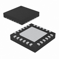
ATA8742-PXQW Atmel, ATA8742-PXQW Datasheet - Page 76

ATA8742-PXQW
Manufacturer Part Number
ATA8742-PXQW
Description
MCU W/TRANSMITTER ASK/FSK 24QFN
Manufacturer
Atmel
Datasheet
1.ATA8742-PXQW.pdf
(238 pages)
Specifications of ATA8742-PXQW
Frequency
433MHz
Applications
Home Automation, Remote Sensing, RKE
Modulation Or Protocol
ASK, FSK
Data Rate - Maximum
32 kBit/s
Power - Output
7.5dBm
Current - Transmitting
9.8mA
Data Interface
PCB, Surface Mount
Antenna Connector
PCB, Surface Mount
Memory Size
4kB Flash, 256B EEPROM, 256B SRAM
Voltage - Supply
2 V ~ 4 V
Operating Temperature
-40°C ~ 85°C
Package / Case
24-VQFN Exposed Pad, 24-HVQFN, 24-SQFN, 24-DHVQFN
Processor Series
ATA8x
Core
AVR8
Data Bus Width
8 bit
Program Memory Type
Flash
Program Memory Size
4 KB
Data Ram Size
256 B
Interface Type
SPI, USI
Maximum Clock Frequency
8.1 MHz
Number Of Programmable I/os
12
Number Of Timers
2
Maximum Operating Temperature
+ 85 C
Mounting Style
SMD/SMT
Development Tools By Supplier
ATASTK512-EK1-IND
Minimum Operating Temperature
- 40 C
On-chip Adc
10 bit, 8 Channel
Lead Free Status / RoHS Status
Lead free / RoHS Compliant
Features
-
Lead Free Status / Rohs Status
Details
Available stocks
Company
Part Number
Manufacturer
Quantity
Price
Company:
Part Number:
ATA8742-PXQW
Manufacturer:
ATMEL
Quantity:
1 482
- Current page: 76 of 238
- Download datasheet (4Mb)
19.2.5
76
ATA8742
Digital Input Enable and Sleep Modes
are read back again, but as previously discussed, a nop instruction is included to be able to read
back the value recently assigned to some of the pins.
Note:
As shown in
input of the schmitt-trigger. The signal denoted SLEEP in the figure, is set by the MCU Sleep
Controller in Power-down mode, Power-save mode, and Standby mode to avoid high power
consumption if some input signals are left floating, or have an analog signal level close to V
SLEEP is overridden for port pins enabled as external interrupt pins. If the external interrupt
request is not enabled, SLEEP is active also for these pins. SLEEP is also overridden by various
other alternate functions as described in
If a logic high level (“one”) is present on an asynchronous external interrupt pin configured as
“Interrupt on Rising Edge, Falling Edge, or Any Logic Change on Pin” while the external interrupt
is not enabled, the corresponding External Interrupt Flag will be set when resuming from the
above mentioned Sleep mode, as the clamping in these sleep mode produces the requested
logic change.
Assembly Code Example
C Code Example
unsigned char i;
...
; Define pull-ups and set outputs high
; Define directions for port pins
ldi
ldi
out
out
; Insert nop for synchronization
nop
; Read port pins
in
...
...
/* Define pull-ups and set outputs high */
/* Define directions for port pins */
PORTA = (1<<PA4)|(1<<PA1)|(1<<PA0);
DDRA = (1<<DDA3)|(1<<DDA2)|(1<<DDA1)|(1<<DDA0);
/* Insert nop for synchronization*/
_NOP();
/* Read port pins */
i = PINA;
...
1. For the assembly program, two temporary registers are used to minimize the time from
pull-ups are set on pins 0, 1 and 4, until the direction bits are correctly set, defining bit 2 and 3
as low and redefining bits 0 and 1 as strong high drivers.
Figure 19-2 on page
r16,(1<<PA4)|(1<<PA1)|(1<<PA0)
r17,(1<<DDA3)|(1<<DDA2)|(1<<DDA1)|(1<<DDA0)
PORTA,r16
DDRA,r17
r16,PINA
(1)
73, the digital input signal can be clamped to ground at the
“Alternate Port Functions” on page
77.
9151A–INDCO–07/09
CC
/2.
Related parts for ATA8742-PXQW
Image
Part Number
Description
Manufacturer
Datasheet
Request
R

Part Number:
Description:
Manufacturer:
ATMEL Corporation
Datasheet:

Part Number:
Description:
DEV KIT FOR AVR/AVR32
Manufacturer:
Atmel
Datasheet:

Part Number:
Description:
INTERVAL AND WIPE/WASH WIPER CONTROL IC WITH DELAY
Manufacturer:
ATMEL Corporation
Datasheet:

Part Number:
Description:
Low-Voltage Voice-Switched IC for Hands-Free Operation
Manufacturer:
ATMEL Corporation
Datasheet:

Part Number:
Description:
MONOLITHIC INTEGRATED FEATUREPHONE CIRCUIT
Manufacturer:
ATMEL Corporation
Datasheet:

Part Number:
Description:
AM-FM Receiver IC U4255BM-M
Manufacturer:
ATMEL Corporation
Datasheet:

Part Number:
Description:
Monolithic Integrated Feature Phone Circuit
Manufacturer:
ATMEL Corporation
Datasheet:

Part Number:
Description:
Multistandard Video-IF and Quasi Parallel Sound Processing
Manufacturer:
ATMEL Corporation
Datasheet:

Part Number:
Description:
High-performance EE PLD
Manufacturer:
ATMEL Corporation
Datasheet:

Part Number:
Description:
8-bit Flash Microcontroller
Manufacturer:
ATMEL Corporation
Datasheet:

Part Number:
Description:
2-Wire Serial EEPROM
Manufacturer:
ATMEL Corporation
Datasheet:


