WM8986GECO/V Wolfson Microelectronics, WM8986GECO/V Datasheet
WM8986GECO/V
Specifications of WM8986GECO/V


Related parts for WM8986GECO/V

WM8986GECO/V Summary of contents
Page 1
... Low power, low voltage • 2.5V to 3.6V analogue supplies • 1.71V to 3.6V digital supplies • 4x4mm 28-lead COL QFN package APPLICATIONS • Portable audio player / FM radio • Multimedia Mobile Handsets http://www.wolfsonmicro.com/enews/ WM8986 Production Data, June 2009, Rev 4.1 Copyright ©2008 Wolfson Microelectronics plc ...
Page 2
WM8986 BLOCK DIAGRAM w Production Data PD, Rev 4.1, June 2009 2 ...
Page 3
Production Data DESCRIPTION ....................................................................................................... 1 FEATURES............................................................................................................. 1 APPLICATIONS ..................................................................................................... 1 BLOCK DIAGRAM ................................................................................................. 2 TABLE OF CONTENTS ......................................................................................... 3 PIN CONFIGURATION ........................................................................................... 4 ORDERING INFORMATION .................................................................................. 4 PIN DESCRIPTION ................................................................................................ 5 ABSOLUTE MAXIMUM RATINGS ......................................................................... 6 RECOMMENDED OPERATING CONDITIONS ..................................................... ...
Page 4
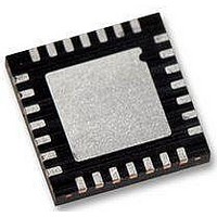
... WM8986 PIN CONFIGURATION ORDERING INFORMATION ORDER CODE TEMPERATURE RANGE WM8986GECO/V -40°C to +85°C WM8986GECO/RV -40°C to +85°C Note: Reel quantity = 3,500 w PACKAGE SENSITIVITY LEVEL 28-lead COL QFN ( mm) (Pb-free) 28-lead COL QFN ( mm) (Pb-free, tape and reel) Production Data MOISTURE PEAK SOLDERING TEMPERATURE ...
Page 5
Production Data PIN DESCRIPTION PIN NAME 1 LIP Analogue input Analogue input 2 LIN 3 RIP Analogue input 4 RIN Analogue input 5 DACDAT Digital Input 6 LRC Digital Input / Output 7 BCLK Digital Input / Output 8 MCLK ...
Page 6
WM8986 ABSOLUTE MAXIMUM RATINGS Absolute Maximum Ratings are stress ratings only. Permanent damage to the device may be caused by continuously operating at or beyond these limits. Device functional operating limits and guaranteed performance specifications are given under Electrical Characteristics ...
Page 7
Production Data ELECTRICAL CHARACTERISTICS Test Conditions DCVDD=1.8V, AVDD1=AVDD2=DBVDD=3.3V, T PARAMETER Microphone Input PGA Inputs (LIP, LIN, RIP, RIN) INPPGAVOLL, INPPGAVOLR, PGABOOSTL and PGABOOSTR = 0dB Full-scale Input Signal Level – 1 Single-ended input via LIN/RIN Full-scale Input Signal Level – ...
Page 8
WM8986 Test Conditions DCVDD=1.8V, AVDD1=AVDD2=DBVDD=3.3V, T PARAMETER DAC to left and right mixers into 10kΩ / 50pF load on LOUT1 and ROUT1 LOUT1VOL, ROUT1VOL, DACLVOL and DACRVOL = 0dB 1 Full-scale output 3 Signal to Noise Ratio 4 Total Harmonic ...
Page 9
Production Data Test Conditions DCVDD=1.8V, AVDD1=AVDD2=DBVDD=3.3V, T PARAMETER 6 Channel Separation DAC to left and right mixer into headphone (16Ω load on LOUT1 and ROUT1 LOUT1VOL, ROUT1VOL, DACLVOL and DACRVOL = 0dB Full-scale output 3 Signal to Noise Ratio 4 ...
Page 10
WM8986 Test Conditions DCVDD=1.8V, AVDD1=AVDD2=DBVDD=3.3V, T PARAMETER AUXL and AUXR into on OUT3/OUT4 outputs on 10kΩ / 50pF load INPPGAVOLL, INPPGAVOLR = 0dB Full-scale output voltage, 0dB gain 3 Signal to Noise Ratio 4 Total Harmonic Distortion 5 Total Harmonic ...
Page 11
Production Data Test Conditions DCVDD=1.8V, AVDD1=AVDD2=DBVDD=3.3V, T PARAMETER Digital Input / Output Input HIGH Level Input LOW Level Output HIGH Level Output LOW Level Input Capacitance Input leakage TERMINOLOGY 1. Full-scale input and output levels scale in relation to AVDD ...
Page 12
WM8986 POWER CONSUMPTION Typical power consumption for various scenarios is shown below. All measurements are made with quiescent signal. Description Off (Default Settings) Standby mode (Lowest Power) DAC Playback 32Ω load L/ROUT2 - Class AB Mode fs=44.1kHz Table 1 Power ...
Page 13
Production Data AUDIO PATHS OVERVIEW Figure 1 Audio Paths Overview w WM8986 PD, Rev 4.1, June 2009 13 ...
Page 14
WM8986 SIGNAL TIMING REQUIREMENTS SYSTEM CLOCK TIMING MCLK Figure 2 System Clock Timing Requirements Test Conditions DCVDD=1.8V, DBVDD=AVDD1=AVDD2=3.3V, DGND=AGND1=AGND2=0V, T PARAMETER System Clock Timing Information MCLK cycle time MCLK duty cycle Note: 1. PLL pre-scaling and PLL N and K ...
Page 15
Production Data Test Conditions DCVDD=1.8V, DBVDD=AVDD1=AVDD2=3.3V, DGND=AGND1=AGND2=0V, T MCLK=256fs, 24-bit data, unless otherwise stated. PARAMETER Audio Data Input Timing Information LRC propagation delay from BCLK falling edge DACDAT setup time to BCLK rising edge DACDAT hold time from BCLK rising ...
Page 16
WM8986 CONTROL INTERFACE TIMING – 3-WIRE MODE 3-wire mode is selected by connecting the MODE pin high. Figure 5 Control Interface Timing – 3-Wire Serial Control Mode Test Conditions DCVDD = 1.8V, DBVDD = AVDD1 = AVDD2 = 3.3V, DGND ...
Page 17
Production Data CONTROL INTERFACE TIMING – 2-WIRE MODE 2-wire mode is selected by connecting the MODE pin low. SDIN SCLK Figure 6 Control Interface Timing – 2-Wire Serial Control Mode Test Conditions DCVDD=1.8V, DBVDD=AVDD1=AVDD2=3.3V, MCLK = 256fs, 24-bit data, unless ...
Page 18
WM8986 INTERNAL POWER ON RESET CIRCUIT Figure 7 Internal Power on Reset Circuit Schematic The WM8986 includes an internal Power-On-Reset Circuit, as shown in Figure 7, which is used to reset the digital logic into a default state after power ...
Page 19
Production Data Figure 9 Typical Power up Sequence where DCVDD is Powered before AVDD1 Figure 9 shows a typical power-up sequence where DCVDD comes up first. First it is assumed that DCVDD is already up to specified operating voltage. When ...
Page 20
WM8986 RECOMMENDED POWER UP/DOWN SEQUENCE In order to minimise output pop and click noise recommended that the WM8986 device is powered up and down under control using the following sequences: Power Up: 1. Turn on external power supplies. ...
Page 21
Production Data Figure 10 DAC Power Up and Down Sequence (not to scale) SYMBOL t line_midrail_on t line_midrail_off t hp_midrail_on t hp__midrail_off t dacint DAC Group Delay Table 3 Typical POR Operation (Typical Simulated Values) Notes: 1. The lineout charge ...
Page 22
WM8986 DEVICE DESCRIPTION INTRODUCTION The WM8986 is a low power audio IC combining a high quality stereo audio DAC with flexible line and microphone input and output processing. FEATURES The chip offers great flexibility in use, and so can support ...
Page 23
Production Data Selection of the mode is via the MODE pin wire mode, the address of the device is fixed as 0011010. CLOCKING SCHEMES WM8986 offers the normal audio DAC clocking scheme operation, where 256fs MCLK is provided ...
Page 24
WM8986 Figure 11 Microphone Input PGA Circuit In single-ended microphone input configuration the microphone signal should be input to LIN or RIN and the non-inverting input of the input PGA clamped to VMID. GND MIC MICBIAS Figure 12 Psuedo-Differential Microphone ...
Page 25
Production Data MICBIAS MIC GND Figure 13 Single-ended Microphone Configuration The input PGAs are enabled by the INPPGAENL and INPPGAENR register bits. REGISTER ADDRESS R2 (02h) Power Management 2 Table 4 Input PGA Enable Register Settings REGISTER ADDRESS R44 (2Ch) ...
Page 26
WM8986 INPUT PGA VOLUME CONTROLS The input microphone PGAs have a gain range from -12dB to +35.25dB in 0.75dB steps. The gain from the LIN/RIN input to the PGA output is controlled by the register bits INPPGAVOLL[5:0] and INPPGABVOLR[5:0]. These ...
Page 27
Production Data VOLUME UPDATES Volume settings will not be applied to the PGAs until a '1' is written to one of the INPPGAVU bits. This is to allow left and right channels to be updated at the same time, as ...
Page 28
WM8986 Figure 16 Volume Update Using Zero Cross Detection If there is a long period where no zero-crossing occurs, a timeout circuit in the WM8986 will automatically update the volume. The volume updates will occur between one and two timeout ...
Page 29
Production Data AUXILIARY INPUTS There are two auxiliary inputs, AUXL and AUXR which can be used for a variety of purposes such as stereo line inputs ‘beep’ input signal to be mixed with the outputs. The AUXL/R ...
Page 30
WM8986 The input PGA paths can have a +20dB boost (PGABOOSTL/R=1), a 0dB pass through (PGABOOSTL/R= completely isolated from the input boost circuit (INPPGAMUTEL/R=1). REGISTER ADDRESS R47 (2Fh) Left Input BOOST control R48 (30h) Right Input BOOST control ...
Page 31
Production Data The BOOST stage is enabled under control of the BOOSTEN register bit. REGISTER ADDRESS R2 (02h) Power management 2 Table 9 Input BOOST Enable Control OUTPUT SIGNAL PATH The WM8986 output signal paths consist of digital application filters, ...
Page 32
WM8986 REGISTER ADDRESS R10 (0Ah) DAC Control Table 11 DAC Control Register The digital audio data is converted to oversampled bit streams in the on-chip, true 24-bit digital interpolation filters. The bitstream data enters the multi-bit, sigma-delta DACs, which convert ...
Page 33
Production Data Note: An additional gain 12dB can be added using the gain block embedded in the digital peak limiter circuit (see DAC OUTPUT LIMITER section). 5-BAND EQUALISER A 5-band graphic equaliser function which can be used ...
Page 34
WM8986 REGISTER ADDRESS R24 (18h) DAC digital limiter control 1 R25 (19h) DAC digital limiter control 2 w BIT LABEL DEFAULT 3:0 LIMATK 0010 7:4 LIMDCY 0011 8 LIMEN 0 3:0 LIMBOOST 0000 Production Data DESCRIPTION Limiter Attack time (per ...
Page 35
Production Data REGISTER ADDRESS Table 13 DAC Digital Limiter Control 5-BAND GRAPHIC EQUALISER A 5-band graphic equaliser is provided, which can be applied to the DAC path, together with 3D enhancement, under control of the EQ3DEN register bit. REGISTER ADDRESS ...
Page 36
WM8986 REGISTER ADDRESS R20 (14h) EQ Band 3 Control Table 17 EQ Band 3 Control REGISTER ADDRESS R21 (15h) EQ Band 4 Control Table 18 EQ Band 4 Control REGISTER ADDRESS R22 (16h) EQ Band 5 Gain Control Table 19 ...
Page 37
Production Data 3D STEREO ENHANCEMENT The WM8986 has a digital 3D enhancement option to increase the perceived separation between the left and right channels. The DEPTH3D setting controls the degree of stereo expansion. REGISTER ADDRESS R41 (29h) 3D Control Table ...
Page 38
WM8986 Figure 21 Left/Right Output Channel Mixers w Production Data PD, Rev 4.1, June 2009 38 ...
Page 39
Production Data REGISTER ADDRESS R43 (2Bh) Output mixer control R43 (2Bh) Output mixer control R49 (31h) Output mixer control R50 (32h) Left channel output mixer control w BIT LABEL DEFAULT 8 BYPL2RMIX 0 7 BYPR2LMIX 0 5 DACR2LMIX 0 6 ...
Page 40
WM8986 REGISTER ADDRESS R51 (33h) Right channel output mixer control R3 (03h) Power management 3 Table 22 Left and Right Output Mixer Control HEADPHONE OUTPUTS (LOUT1 AND ROUT1) The headphone outputs LOUT1 and ROUT1 can drive a 16Ω or 32Ω ...
Page 41
Production Data Headphone Output using DC Blocking Capacitors DC Coupled Headphone Output Figure 22 Recommended Headphone Output Configurations When DC blocking capacitors are used, their capacitance and the load resistance together determine the lower cut-off frequency of the output signal, ...
Page 42
WM8986 REGISTER ADDRESS R52 (34h) LOUT1 Volume control R53 ROUT1 Volume control Table 23 OUT1 Volume Control w BIT LABEL DEFAULT 5:0 LOUT1VOL 111001 (0dB) 6 LOUT1MUTE 0 7 LOUT1ZC 0 8 HPVU Not latched 5:0 ROUT1VOL 111001 (0dB) 6 ...
Page 43
Production Data CLASS D / CLASS AB HEADPHONE OUTPUTS (LOUT2 AND ROUT2) The outputs LOUT2 and ROUT2 are designed to drive two headphone loads of 16Ω or 32Ω or line outputs (See Headphone Output and Line Output sections, respectively). Each ...
Page 44
WM8986 Figure 24 LOUT2 and ROUT2 Class AB Headphone Configuration The output configurations shown in Figure 23 and Figure 24 are both suitable for class AB operation. The signal output on LOUT2/ROUT2 comes from the Left/Right Mixer circuits and can ...
Page 45
Production Data REGISTER ADDRESS R54 (36h) LOUT2 Volume control R55 (37h) ROUT2 Volume control Table 25 OUT2 Volume Control ZERO CROSS TIMEOUT A zero-cross timeout function is provided so that if zero cross is enabled on the input or output ...
Page 46
WM8986 OUT3/OUT4 MIXERS AND OUTPUT STAGES The OUT3/OUT4 pins provide an additional stereo line output, a mono output differential output. There is a dedicated analogue mixer for OUT3 and one for OUT4 as shown in Figure 25. The ...
Page 47
Production Data REGISTER ADDRESS R56 (38h) OUT3 mixer control R57 (39h) OUT4 mixer control Table 27 OUT3/OUT4 Mixer Registers w BIT LABEL DEFAULT 6 OUT3MUTE 0 3 OUT4_2OUT3 0 2 BYPL2OUT3 0 1 LMIX2OUT3 0 0 LDAC2OUT3 1 7 OUT3_2OUT4 ...
Page 48
WM8986 ENABLING THE OUTPUTS Each analogue output of the WM8986 can be independently enabled or disabled. The analogue mixer associated with each output has a separate enable bit. All outputs are disabled by default. To save power, unused parts of ...
Page 49
Production Data REGISTER ADDRESS R49 (31h) Table 30 Disabled Outputs to VREF Resistance A dedicated buffer is available for biasing unused analogue I/O pins as shown in Figure 26. This buffer can be enabled using the BUFIOEN register bit. Figure ...
Page 50
WM8986 DIGITAL AUDIO INTERFACES The audio interface has three pins: • • • The clock signals BCLK, and LRC can be outputs when the WM8986 operates as a master, or inputs when slave (see Master and Slave ...
Page 51
Production Data mode, the MSB is available on the second rising edge of BCLK following a LRC transition. The other bits up to the LSB are then transmitted in order. Depending on word length, BCLK frequency ...
Page 52
WM8986 Figure 32 DSP/PCM Mode Audio Interface (mode A, LRP=0, Slave) Figure 33 DSP/PCM Mode Audio Interface (mode B, LRP=0, Slave) w Production Data PD, Rev 4.1, June 2009 52 ...
Page 53
Production Data REGISTER ADDRESS R4 (04h) Audio Interface Control Table 32 Audio Interface Control Note: Right Justified Mode will only operate with a maximum of 24 bits. If 32-bit mode is selected the device will operate in 24-bit mode. AUDIO ...
Page 54
WM8986 REGISTER ADDRESS R6 (06h) Clock Generation Control Table 33 Clock Control The CLKSEL bit selects the internal source of the Master clock from the PLL (CLKSEL=1) or from MCLK (CLKSEL=0). When the internal clock is switched from one source ...
Page 55
Production Data R7 (07h) Additional Control Table 45 Sample Rate Control MASTER CLOCK AND PHASE LOCKED LOOP (PLL) The WM8986 has an on-chip phase-locked loop (PLL) circuit that can be used to: Generate master clocks for the WM8986 audio functions ...
Page 56
WM8986 selectable divide by N after the PLL which should be set to divide meet this requirement. Enabling the divide by 2 sets the required 12.288MHz = 98.304MHz ...
Page 57
Production Data REGISTER ADDRESS R36 (24h) PLL N value R37 (25h) PLL K value 1 R38 (26h) PLL K Value 2 R39 (27h) PLL K Value 3 Table 47 PLL Frequency Ratio Control The PLL performs best when f are ...
Page 58
WM8986 COMPANDING The WM8986 supports A-law and μ-law companding. Companding can be enabled on the DAC audio interface by writing the appropriate value to the DAC_COMP register bit. REGISTER ADDRESS R5 (05h) Companding Control Table 49 Companding Control Companding involves ...
Page 59
Production Data 120 100 Figure 39 μ-Law Companding 120 100 Figure 40 A-Law Companding w u-law Companding 0.1 0.2 0.3 0.4 Normalised Input A-law Companding 0 0 0.2 0.4 Normalised ...
Page 60
WM8986 GENERAL PURPOSE INPUT/OUTPUT The WM8986 has one dual purpose input/output pin, CSB/GPIO1. The GPIO1 function is provided for use as jack detection input or general purpose output. The default configuration for the CSB/GPIO1 input. When ...
Page 61
Production Data For further details of the jack detect operation see the OUTPUT SWITCHING section. OUTPUT SWITCHING (JACK DETECT) When the device is operated using a 2-wire interface the CSB/GPIO1 pin can be used as a switch control input to ...
Page 62
WM8986 REGISTER ADDRESS R9 (09h) GPIO control R13 (00h) Table 35 Jack Detect Register Control Bits CONTROL INTERFACE SELECTION OF CONTROL MODE AND 2-WIRE MODE ADDRESS The control interface can operate as either a 3-wire or 2-wire control interface. The ...
Page 63
Production Data 2-WIRE SERIAL CONTROL MODE The WM8986 supports software control via a 2-wire serial bus. Many devices can be controlled by the same bus, and each device has a unique 7-bit device address (this is not the same as ...
Page 64
WM8986 POWER MANAGEMENT SAVING POWER BY REDUCING OVERSAMPLING RATE The default mode of operation of the DAC digital filters is in 64x oversampling mode. Under the control of DACOSR128 the oversampling rate may be doubled. 64x oversampling results in a ...
Page 65
Production Data REGISTER MAP REGISTER B8 ADDR NAME B[15:9] DEC HEX 00 0 Software Reset 1 01 Power manage’ Power manage’t 2 ROUT1EN 3 03 Power manage’t 3 OUT4EN 4 04 Audio Interface BCP 5 05 ...
Page 66
WM8986 REGISTER B8 ADDR NAME B[15:9] DEC HEX 45 2D Left INP PGA gain INPGAVU ctrl 46 2E Right INP PGA INPGAVU gain ctrl 47 2F Left Input BOOST PGA control BOOSTL 48 30 Right Input BOOST PGA control BOOSTR ...
Page 67
Production Data REGISTER BITS BY ADDRESS Notes: 1. Default values of N/A indicate non-latched data bits (e.g. software reset or volume update bits). 2. Register bits marked as "Reserved" should not be changed from the default. REGISTER BIT LABEL ADDRESS ...
Page 68
WM8986 REGISTER BIT LABEL ADDRESS 3 (03h) 8 OUT4EN 7 OUT3EN 6 ROUT2EN 5 LOUT2EN 4 3 RMIXEN 2 LMIXEN 1 DACENR 0 DACENL 4 (04h) 8 BCP 7 LRP 6:5 WL 4:3 FMT 2 DLRSWAP 1 0 MONO 5 ...
Page 69
Production Data REGISTER BIT LABEL ADDRESS 5 WL8 4:3 DAC_COMP 2:0 6 (06h) 8 CLKSEL 7:5 MCLKDIV 4:2 BCLKDIV (07h) 8 M128ENB 7:4 DCLKDIV w DEFAULT DESCRIPTION 0 Companding Control 8-bit mode 0=off 1=device operates in ...
Page 70
WM8986 REGISTER BIT LABEL ADDRESS 3 SLOWCLKEN 8 (08h) 8 GPIO1GP 7 GPIO1GPU 6 GPIO1GPD 3 GPIO1POL 2:0 GPIO1SEL [2:0] 9 (09h) 8:7 6 JD_EN 5:0 10 (0Ah) 8:7 6 SOFTMUTE 5:4 3 DACOSR128 w DEFAULT DESCRIPTION 000 ...
Page 71
Production Data REGISTER BIT LABEL ADDRESS 2 AMUTE 1 DACPOLR 0 DACPOLL 11 (0Bh) 8 DACVU 7:0 DACVOLL 12 (0Ch) 8 DACVU 7:0 DACVOLR 13 (0Dh) 8 7:4 JD_EN1 3:0 JD_EN0 14 (0Eh) 5:4 OPCLKDIV 15 (0Fh) 8:0 16 (10h) ...
Page 72
WM8986 REGISTER BIT LABEL ADDRESS 19 (13h) 8 EQ2BW 7 6:5 EQ2C 4:0 EQ2G 20 (14h) 8 EQ3BW 7 6:5 EQ3C 4:0 EQ3G 21 (15h) 8 EQ4BW 7 6:5 EQ4C 4:0 EQ4G 22 (16h) 8:7 6:5 EQ5C 4:0 EQ5G 23 ...
Page 73
Production Data REGISTER BIT LABEL ADDRESS 7:4 LIMDCY 3:0 LIMATK 25 (19h) 8:7 6:4 LIMLVL 3:0 LIMBOOST 27 (1Bh) 8:0 28 (1Ch) 8:0 29 (1Dh) 8:0 30 (1Eh) 8:0 32 (20h) 8:0 33 (21h) 8:0 w DEFAULT DESCRIPTION 0011 DAC ...
Page 74
WM8986 REGISTER BIT LABEL ADDRESS 34 (22h) 8:0 35 (23h) 8:0 36 (24h) 8:5 4 PLL PRESCALE 3:0 PLLN[3:0] 37 (25h) 8:6 5:0 PLLK[23:18] 38 (26h) 8:0 PLLK[17:9] 39 (27h) 8:0 PLLK[8:0] 41 (29h) 8:4 3:0 DEPTH3D 42 (2Ah) 8:3 ...
Page 75
Production Data REGISTER BIT LABEL ADDRESS 4 RIP2INPPGA LIN2INPPGA 0 LIP2INPPGA 45 (2Dh) 8 INPPGAU 7 INPPGAZCL 6 INPPGAMUTEL 5:0 INPPGAVOLL 46 (2Eh) 8 INPPGAU 7 INPPGAZCR 6 INPPGAMUTER 5:0 INPPGAVOLR w DEFAULT DESCRIPTION 1 Connect RIP ...
Page 76
WM8986 REGISTER BIT LABEL ADDRESS 47 (2Fh) 8 PGABOOSTL 7:3 2:0 AUXL2BOOSTVOL 48 (30h) 8 PGABOOSTR 7:3 2:0 AUXR2BOOSTVOL 49 (31h) 8:7 6 DACL2RMIX 5 DACR2LMIX 4:3 2 TSOPCTRL 1 TSDEN 0 VROI 50 (32h) 8:6 AUXLMIXVOL w DEFAULT DESCRIPTION ...
Page 77
Production Data REGISTER BIT LABEL ADDRESS 5 AUXL2LMIX 4:2 BYPLMIXVOL 1 BYPL2L MIX 0 DACL2L MIX 51 (33h) 8:6 AUXRMIXVOL 5 AUXR2RMIX 4:2 BYPRMIXVOL 1 BYPR2RMIX 0 DACR2RMIX 52 (34h) 8 OUT1VU 7 LOUT1ZC 6 LOUT1MUTE w DEFAULT DESCRIPTION 0 ...
Page 78
WM8986 REGISTER BIT LABEL ADDRESS 5:0 LOUT1VOL 53 (35h) 8 OUT1VU 7 ROUT1ZC 6 ROUT1MUTE 5:0 ROUT1VOL 54 (36h) 8 OUT2VU 7 LOUT2ZC 6 LOUT2MUTE 5:0 LOUT2VOL 55 (37h) 8 OUT2VU 7 ROUT2ZC 6 ROUT2MUTE 5:0 ROUT2VOL 56 (38h) 8:7 ...
Page 79
Production Data REGISTER BIT LABEL ADDRESS 3 OUT4_2OUT3 2 BYPL2OUT3 1 LMIX2OUT3 0 LDAC2OUT3 57 (39h OUT3_2OUT4 6 OUT4MUTE 5 HALFSIG 4 LMIX2OUT4 3 LDAC2OUT4 2 BYPR2OUT4 1 RMIX2OUT4 0 RDAC2OUT4 61 (3Dh) 8 7:0 w DEFAULT DESCRIPTION ...
Page 80
WM8986 DAC DIGITAL FILTER CHARACTERISTICS PARAMETER Passband Passband Ripple Stopband Stopband Attenuation Group Delay Table 43 DAC Digital Filter Characteristics TERMINOLOGY 1. Stop Band Attenuation (dB) – the degree to which the frequency spectrum is attenuated (outside audio band) 2. ...
Page 81
Production Data DAC FILTER RESPONSES 20 0 -20 -40 -60 -80 -100 -120 -140 -160 0 0.5 1 Frequency (fs) Figure 36 DAC Digital Filter Frequency Response (128xOSR -20 -40 -60 -80 -100 -120 -140 -160 0 0.5 ...
Page 82
WM8986 5-BAND EQUALISER The WM8986 has a 5-band equaliser which can be applied to either the ADC path or the DAC path. The plots from Figure 40 to Figure 53 show the frequency responses of each filter with a sampling ...
Page 83
Production Data -10 - Frequency (Hz) Figure 45 EQ Band 3 – Peak Filter Centre Frequencies, EQ3BFigure -10 - ...
Page 84
WM8986 -10 - Frequency (Hz) Figure 48 EQ Band 4 – Peak Filter Centre Frequencies, EQ3BFigure -10 - ...
Page 85
Production Data Figure 53 shows the result of having the gain set on more than one channel simultaneously. The blue traces show each band (lowest cut-off/centre frequency) with ±12dB gain. The red traces show the cumulative effect of all bands ...
Page 86
WM8986 APPLICATIONS INFORMATION RECOMMENDED EXTERNAL COMPONENTS Figure 54 External Component Diagram Notes: 1. When operating LOUT2 and ROUT2 in class D mode recommended that LC filtering is placed as close to the LOUT2 and ROUT2 pins as possible. ...
Page 87
Production Data PACKAGE DIAGRAM FL: 28 PIN COL QFN PLASTIC PACKAGE BOTTOM VIEW A3 C SIDE VIEW SEATING PLANE Exposed lead Dimensions (mm) Symbols NOM MIN ...
Page 88
... WM8986 IMPORTANT NOTICE Wolfson Microelectronics plc (“Wolfson”) products and services are sold subject to Wolfson’s terms and conditions of sale, delivery and payment supplied at the time of order acknowledgement. Wolfson warrants performance of its products to the specifications in effect at the date of shipment. Wolfson reserves the right to make changes to its products and specifications or to discontinue any product or service without notice ...