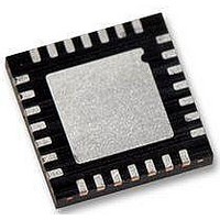
WM8986GECO/V Wolfson Microelectronics, WM8986GECO/V Datasheet - Page 9

WM8986GECO/V
Manufacturer Part Number
WM8986GECO/V
Description
Audio Amplifiers Class D Headphone DAC + Line Out
Manufacturer
Wolfson Microelectronics
Datasheet
1.WM8986GECOV.pdf
(88 pages)
Specifications of WM8986GECO/V
Product
Class-D
Output Power
40 mW
Thd Plus Noise
- 86 dB
Operating Supply Voltage
1.71 V to 3.6 V, 2.5 V to 3.6 V
Maximum Operating Temperature
+ 85 C
Mounting Style
SMD/SMT
Audio Load Resistance
16 Ohms
Minimum Operating Temperature
- 40 C
Output Signal Type
Differential
Supply Voltage (max)
3.6 V
Supply Voltage (min)
1.71 V, 2.5 V
Output Type
Differential
Package / Case
QFN-28
Lead Free Status / RoHS Status
Lead free / RoHS Compliant
Production Data
w
Test Conditions
DCVDD=1.8V, AVDD1=AVDD2=DBVDD=3.3V, T
PARAMETER
Channel Separation
DAC to left and right mixer into headphone (16Ω load on LOUT1 and ROUT1
LOUT1VOL, ROUT1VOL, DACLVOL and DACRVOL = 0dB
Full-scale output
Signal to Noise Ratio
Total Harmonic Distortion
Total Harmonic Distortion + Noise
Channel Separation
DAC to left and right mixer into headphone (16Ω load) on LOUT2 and ROUT2, Class AB mode
LOUT2VOL, ROUT2VOL, DACLVOL and DACRVOL = 0dB
Full-scale output
Signal to Noise Ratio
Total Harmonic Distortion
Total Harmonic Distortion + Noise
Channel Separation
DAC to left and right mixer into headphone load on LOUT2 and ROUT2, Class D mode, L
LOUT2VOL, ROUT2VOL, DACLVOL and DACRVOL = 0dB
Full-scale output
Signal to Noise Ratio
Total Harmonic Distortion
Total Harmonic Distortion + Noise
Channel Separation
PWM Rise Time
PWM Fall Time
PWM Switching Frequency
Efficiency
Power Supply Rejection
Idle Current
PGA outputs to left and right output mixers. BYPL2LMIX = 1 and BYPR2RMIX = 1
PGA gain range into mixer
BYPLMIXVOL and BYPRMIXVOL
gain step into mixer
Mute attenuation
Analogue outputs (LOUT1, ROUT1, LOUT2, ROUT2)
Programmable Gain range
Programmable Gain step size
Mute attenuation
6
6
6
6
3
3
3
4
4
4
5
5
5
SYMBOL
THD+N
THD+N
THD+N
PSRR
SNR
THD
SNR
THD
SNR
THD
A
= +25
No analogue output signal
R
P
100mV
O
L
AVDD1=AVDD2=2.5V
Po = 20mW, RL=16Ω
1kHz, full scale signal
P
P
P
P
L/ROUT2VOL = 0dB
P
o
TEST CONDITIONS
L/ROUT1MUTE = 1
L/ROUT2MUTE = 1
= 16Ω, t
injected on AVDD2
= 20mW
BYPLMIXVOL and
L/ROUT1VOL and
C, 1kHz signal, fs = 48kHz, 24-bit audio data unless otherwise stated.
o
o
o
o
o
DCLKDIV = 1000
on either channel
Gain adjusted by
BYPR2RMIX = 0
Gain adjusted by
BYPL2LMIX = 0
= 20mW, RL=16Ω
= 20mW, RL=16Ω
= 20mW, RL=16Ω
= 20mW, RL=16Ω
= 20mW, RL=16Ω
22Hz to 20kHz
22Hz to 20kHz
BYPRMIXVOL
L/ROUT2VOL
1kHz signal
1kHz signal
1kHz signal
1kHz signal
A-weighted
A-weighted
A-weighted
Monotonic
pp
ripple @217Hz
PW
= 20ns,
MIN
-15
-57
90
80
AVDD1/3.3
AVDD1/3.3
AVDD1/3.3
filter
95.5
95.5
TYP
100
100
100
100
100
100
-75
-75
-84
-81
-78
-74
1.5
1.5
1.4
0.5
97
90
72
70
85
0
3
0
1
= 33uH C
PD, Rev 4.1, June 2009
filter
MAX
-75
-70
-70
-70
+6
+6
= 220nf
WM8986
UNIT
MHz
V
V
V
mA
dB
dB
dB
dB
dB
dB
dB
dB
dB
dB
dB
dB
dB
dB
dB
dB
dB
dB
dB
dB
dB
dB
ns
ns
%
rms
rms
rms
9


