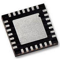
WM8986GECO/V Wolfson Microelectronics, WM8986GECO/V Datasheet - Page 48

WM8986GECO/V
Manufacturer Part Number
WM8986GECO/V
Description
Audio Amplifiers Class D Headphone DAC + Line Out
Manufacturer
Wolfson Microelectronics
Datasheet
1.WM8986GECOV.pdf
(88 pages)
Specifications of WM8986GECO/V
Product
Class-D
Output Power
40 mW
Thd Plus Noise
- 86 dB
Operating Supply Voltage
1.71 V to 3.6 V, 2.5 V to 3.6 V
Maximum Operating Temperature
+ 85 C
Mounting Style
SMD/SMT
Audio Load Resistance
16 Ohms
Minimum Operating Temperature
- 40 C
Output Signal Type
Differential
Supply Voltage (max)
3.6 V
Supply Voltage (min)
1.71 V, 2.5 V
Output Type
Differential
Package / Case
QFN-28
Lead Free Status / RoHS Status
Lead free / RoHS Compliant
WM8986
w
ENABLING THE OUTPUTS
Each analogue output of the WM8986 can be independently enabled or disabled. The analogue
mixer associated with each output has a separate enable bit. All outputs are disabled by default. To
save power, unused parts of the WM8986 should remain disabled.
Outputs can be enabled at any time, but it is not recommended to do so when BUFIO is disabled
(BUFIOEN=0), as this may cause pop noise (see “Power Management” and “Applications
Information” sections).
Table 28 Output Stages Power Management Control
Note: The SLEEP bit R2[6] should only be used when the device is already in Standby mode. The
SLEEP bit prevents the MCLK from propagating round the device when the external MCLK signal
cannot be removed.
THERMAL SHUTDOWN
To protect the WM8986 from becoming too hot, a thermal sensor has been built in. If the device
junction temperature reaches approximately 125°C and the TSDEN and TSOPCTRL bit are set, then
all outputs will be disabled to avoid further increase of the chip temperature.
Additionally, when the device is too hot and TSDEN is set, then the WM8986 de-asserts GPIO bit 11,
a virtual GPIO that can be set up to generate an interrupt to the CPU (see “GPIO and Interrupt
Control” section).
Table 29 Thermal Shutdown
UNUSED ANALOGUE INPUTS/OUTPUTS
Whenever an analogue input/output is disabled, it remains connected to a voltage source (AVDD1/2)
through a resistor. This helps to prevent pop noise when the output is re-enabled. The resistance
between the voltage buffer and the output pins can be controlled using the VROI control bit. The
default impedance is low, so that any capacitors on the outputs can charge up quickly at start-up. If a
high impedance is desired for disabled outputs, VROI can then be set to 1, increasing the resistance
to about 30kΩ.
R1 (01h)
Power
Management
1
R2 (02h)
Power
Management
2
R3 (03h)
Power
Management
3
Note: All “Enable” bits are 1 = ON, 0 = OFF
R49 (31h)
Output Control
REGISTER
ADDRESS
REGISTER
ADDRESS
2
6
7
8
7
6
2
3
5
6
7
8
BIT
1
2
BIT
BUFIOEN
OUT3MIXEN
OUT4MIXEN
ROUT1EN
LOUT1EN
SLEEP
LMIXEN
RMIXEN
LOUT2EN
ROUT2EN
OUT3EN
OUT4EN
TSDEN
TSOPCTRL
LABEL
LABEL
0
0
0
0
0
0
0
0
0
0
0
0
0
0
DEFAULT
DEFAULT
Unused input/output bias buffer enable
OUT3 mixer enable
OUT4 mixer enable
ROUT1 output enable
LOUT1 output enable
0 = Normal device operation
1 = Supply current reduced in device
standby mode when clock supplied (see
Note)
Left mixer enable
Right mixer enable
LOUT2 output enable
ROUT2 output enable
OUT3 enable
OUT4 enable
Thermal Sensor Enable
0 = disabled
1 = enabled
Thermal Shutdown Output enable
0 = Disabled
1 = Enabled, i.e. all outputs will be
disabled if TI set and the device junction
temperature is more than 125ºC.
DESCRIPTION
DESCRIPTION
PD, Rev 4.1, June 2009
Production Data
48


