WM8986GECO/V Wolfson Microelectronics, WM8986GECO/V Datasheet - Page 11
WM8986GECO/V
Manufacturer Part Number
WM8986GECO/V
Description
Audio Amplifiers Class D Headphone DAC + Line Out
Manufacturer
Wolfson Microelectronics
Datasheet
1.WM8986GECOV.pdf
(88 pages)
Specifications of WM8986GECO/V
Product
Class-D
Output Power
40 mW
Thd Plus Noise
- 86 dB
Operating Supply Voltage
1.71 V to 3.6 V, 2.5 V to 3.6 V
Maximum Operating Temperature
+ 85 C
Mounting Style
SMD/SMT
Audio Load Resistance
16 Ohms
Minimum Operating Temperature
- 40 C
Output Signal Type
Differential
Supply Voltage (max)
3.6 V
Supply Voltage (min)
1.71 V, 2.5 V
Output Type
Differential
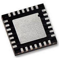
Package / Case
QFN-28
Lead Free Status / RoHS Status
Lead free / RoHS Compliant


Production Data
TERMINOLOGY
1.
2.
3.
4.
5.
6.
w
Test Conditions
DCVDD=1.8V, AVDD1=AVDD2=DBVDD=3.3V, T
PARAMETER
Digital Input / Output
Input HIGH Level
Input LOW Level
Output HIGH Level
Output LOW Level
Input Capacitance
Input leakage
example, when AVDD = 3.3V, 0dBFS = 1V
with a linear relationship to AVDD.
reduced.
device output with no signal applied. This ratio is also called idle channel noise. (No Auto-zero or Automute function is
employed in achieving these results).
first seven odd harmonics of the output signal. To calculate the ratio, the fundamental frequency of the output signal
is notched out and an RMS value of the next seven harmonics is calculated.
signal and the sum of the harmonics, wide-band noise and interference on the output signal. To calculate the ratio,
the fundamental frequency of the output signal is notched out and an RMS value of the total harmonics, wide-band
noise and interference is calculated.
Full-scale input and output levels scale in relation to AVDD or AVDD2 depending upon the input or output used. For
Input level to RIP and LIP in differential configurations is limited to a maximum of -3dB or performance will be
Signal-to-noise ratio (dBFS) – SNR is the difference in level between a reference full scale output signal and the
Total Harmonic Distortion (dBFS) – THD is the difference in level between a reference full scale output signal and the
Total Harmonic Distortion plus Noise (dBFS) – THD+N is the difference in level between a reference full scale output
Channel Separation (dB) – Also known as Cross-Talk. This is a measure of the amount one channel is isolated from
the other. Normally measured by sending a full scale signal down one channel and measuring the other.
SYMBOL
V
V
V
V
OH
OL
IH
IL
rms
A
(0dBV). When AVDD < 3.3V the absolute level of 0dBFS will decrease
= +25
o
TEST CONDITIONS
C, 1kHz signal, fs = 48kHz, 24-bit audio data unless otherwise stated.
All digital pins
I
I
OL
OH
=1mA
-1mA
0.7×DBV
0.9×DBV
MIN
DD
DD
TYP
10
11
PD, Rev 4.1, June 2009
0.3×DBVDD
0.1xDBVDD
MAX
WM8986
UNIT
pF
pA
V
V
V
V
11
Related parts for WM8986GECO/V
Image
Part Number
Description
Manufacturer
Datasheet
Request
R

Part Number:
Description:
Manufacturer:
Wolfson Microelectronics
Datasheet: