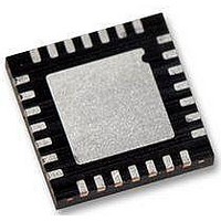
WM8986GECO/V Wolfson Microelectronics, WM8986GECO/V Datasheet - Page 60

WM8986GECO/V
Manufacturer Part Number
WM8986GECO/V
Description
Audio Amplifiers Class D Headphone DAC + Line Out
Manufacturer
Wolfson Microelectronics
Datasheet
1.WM8986GECOV.pdf
(88 pages)
Specifications of WM8986GECO/V
Product
Class-D
Output Power
40 mW
Thd Plus Noise
- 86 dB
Operating Supply Voltage
1.71 V to 3.6 V, 2.5 V to 3.6 V
Maximum Operating Temperature
+ 85 C
Mounting Style
SMD/SMT
Audio Load Resistance
16 Ohms
Minimum Operating Temperature
- 40 C
Output Signal Type
Differential
Supply Voltage (max)
3.6 V
Supply Voltage (min)
1.71 V, 2.5 V
Output Type
Differential
Package / Case
QFN-28
Lead Free Status / RoHS Status
Lead free / RoHS Compliant
WM8986
GENERAL PURPOSE INPUT/OUTPUT
w
The WM8986 has one dual purpose input/output pin, CSB/GPIO1.
The GPIO1 function is provided for use as jack detection input or general purpose output.
The default configuration for the CSB/GPIO1 is to be an input.
When setup as an input, the CSB/GPIO1 pin can either be used as CSB or for jack detection,
depending on how the MODE pin is set.
Table 34 illustrates the functionality of the GPIO1 pin when used as a general purpose output.
Table 34 CSB/GPIO Control
Note: If MODE is set to 3 wire mode, CSB/GPIO1 is used as CSB input irrespective of the
GPIO1SEL[2:0] bits.
R8 (08h)
GPIO
Control
R14(0Eh)
GPIO
Control
REGISTER
ADDRESS
2:0
3
6
7
8
5:4
BIT
GPIO1SEL
GPIO1POL
GPIO1GPD
GPIO1GPU
GPIO1GP
OPCLKDIV
LABEL
000
0
0
0
0
00
DEFAULT
CSB/GPIO1 pin function select:
000 = input (CSB / Jack detection:
depending on MODE setting)
001 = reserved
010 = Temp ok
011 = Amute active
100 = PLL clk output
101 = PLL lock
110 = logic 0
111 = logic 1
GPIO1 Polarity invert
0 = Non inverted
1 = Inverted
GPIO1 Internal pull-down enable:
0 = Internal pull-down disabled
1 = Internal pull-down enabled
GPIO1 Internal pull-up enable:
0 = Internal pull-up disabled
1 = Internal pull-up enabled
GPIO1 Open drain enable
0 = Open drain disabled
1 = Open drain enabled
PLL Output clock division ratio
00 = divide by 1
01 = divide by 2
10 = divide by 3
11 = divide by 4
DESCRIPTION
PD, Rev 4.1, June 2009
Production Data
60


