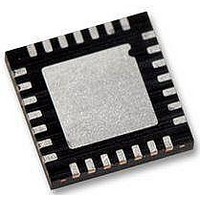
WM8986GECO/V Wolfson Microelectronics, WM8986GECO/V Datasheet - Page 76

WM8986GECO/V
Manufacturer Part Number
WM8986GECO/V
Description
Audio Amplifiers Class D Headphone DAC + Line Out
Manufacturer
Wolfson Microelectronics
Datasheet
1.WM8986GECOV.pdf
(88 pages)
Specifications of WM8986GECO/V
Product
Class-D
Output Power
40 mW
Thd Plus Noise
- 86 dB
Operating Supply Voltage
1.71 V to 3.6 V, 2.5 V to 3.6 V
Maximum Operating Temperature
+ 85 C
Mounting Style
SMD/SMT
Audio Load Resistance
16 Ohms
Minimum Operating Temperature
- 40 C
Output Signal Type
Differential
Supply Voltage (max)
3.6 V
Supply Voltage (min)
1.71 V, 2.5 V
Output Type
Differential
Package / Case
QFN-28
Lead Free Status / RoHS Status
Lead free / RoHS Compliant
WM8986
w
47 (2Fh)
48 (30h)
49 (31h)
50 (32h)
REGISTER
ADDRESS
8
7:3
2:0
8
7:3
2:0
8:7
6
5
4:3
2
1
0
8:6
BIT
PGABOOSTL
AUXL2BOOSTVOL
PGABOOSTR
AUXR2BOOSTVOL
DACL2RMIX
DACR2LMIX
TSOPCTRL
TSDEN
VROI
AUXLMIXVOL
LABEL
1
00000
000
1
00000
000
00
0
0
00
0
1
0
000
DEFAULT
Boost enable for left channel input PGA:
0 = PGA output has +0dB gain through input
BOOST stage.
1 = PGA output has +20dB gain through input
BOOST stage.
Reserved
Controls the auxilliary amplifer to the left channel
input boost stage:
000=Path disabled (disconnected)
001=-12dB gain through boost stage
010=-9dB gain through boost stage
…
111=+6dB gain through boost stage
Boost enable for right channel input PGA:
0 = PGA output has +0dB gain through input
BOOST stage.
1 = PGA output has +20dB gain through input
BOOST stage.
Reserved
Controls the auxilliary amplifer to the right
channel input boost stage:
000=Path disabled (disconnected)
001=-12dB gain through boost stage
010=-9dB gain through boost stage
…
111=+6dB gain through boost stage
Reserved
Left DAC output to right output mixer
0 = not selected
1 = selected
Right DAC output to left output mixer
0 = not selected
1 = selected
Reserved. Initialise to 0
Thermal Shutdown Output enable
0 = Disabled
1 = Enabled, i.e. all outputs will be disabled if TI
set and the device junction temperature is more
than 125ºC.
Thermal Shutdown Enable
0 : thermal shutdown disabled
1 : thermal shutdown enabled
VREF (AVDD/2 or 1.5xAVDD/2) to analogue
output resistance
0: approx 1kΩ
1: approx 30 kΩ
Aux left channel input to left mixer volume
control:
000 = -15dB
001 = -12dB
…
101 = 0dB
110 = +3dB
111 = +6dB
DESCRIPTION
PD, Rev 4.1, June 2009
Input Signal
Path
Input Signal
Path
Input Signal
Path
Input Signal
Path
Analogue
Outputs
Analogue
Outputs
Analogue
Outputs
Analogue
Outputs
Analogue
Outputs
Analogue
Outputs
Production Data
REFER TO
76


