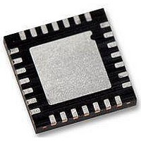
WM8986GECO/V Wolfson Microelectronics, WM8986GECO/V Datasheet - Page 20

WM8986GECO/V
Manufacturer Part Number
WM8986GECO/V
Description
Audio Amplifiers Class D Headphone DAC + Line Out
Manufacturer
Wolfson Microelectronics
Datasheet
1.WM8986GECOV.pdf
(88 pages)
Specifications of WM8986GECO/V
Product
Class-D
Output Power
40 mW
Thd Plus Noise
- 86 dB
Operating Supply Voltage
1.71 V to 3.6 V, 2.5 V to 3.6 V
Maximum Operating Temperature
+ 85 C
Mounting Style
SMD/SMT
Audio Load Resistance
16 Ohms
Minimum Operating Temperature
- 40 C
Output Signal Type
Differential
Supply Voltage (max)
3.6 V
Supply Voltage (min)
1.71 V, 2.5 V
Output Type
Differential
Package / Case
QFN-28
Lead Free Status / RoHS Status
Lead free / RoHS Compliant
WM8986
RECOMMENDED POWER UP/DOWN SEQUENCE
w
In order to minimise output pop and click noise, it is recommended that the WM8986 device is
powered up and down under control using the following sequences:
Power Up:
Power Down
Notes:
1.
2.
3.
4.
5.
6.
7.
8.
9.
10. Setup digital interface, input amplifiers, PLL, and DACs for desired operation.
11. Disable VMID independent current bias, POBCTRL = 0.
12. Unmute L/ROUT1 and set desired volume, e.g. for 0dB R52 and R53 = 0x139h.
13. Unmute L/ROUT2 and set desired volume, e.g. for 0dB R54 and R55 = 0x139h.
1.
2.
3.
4.
5.
1.
2.
3.
Turn on external power supplies. Wait for supply voltage to settle.
Set low analogue bias mode, BIASCUT = 1
Enable thermal shutdown TSDEN = TSOPCTRL = 1
Enable Internal bias BIASEN = 1.
Mute all outputs and set PGAs to minimum gain, R52 to R57 = 0x140h.
Enable VMID independent current bias, POBCTRL = 1.
Enable required outputs, DACs and mixers.
Enable VMID with required charge time e.g. VMIDSEL=01.
Wait 500ms
Disable Thermal shutdown, TSDEN = TSOPCTRL = 0
Disable VMIDSEL=00 and BIASEN=0
Wait for VMID to discharge
Power off registers R1, R2, R3 = 0x000h
Remove external power supplies
Charging time constant is determined by impedance selected by VMIDSEL and the value of
decoupling capacitor connected to VMID pin.
It is possible to interrupt the power down sequence and power up to VMID before the allocated
VMID discharge time. This is done by following the power-up sequence omitting steps 4 to 8.
Discharge time constant is determined by the values of analogue output capacitors.
2
:
1
3
PD, Rev 4.1, June 2009
Production Data
20


