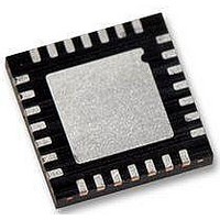
WM8986GECO/V Wolfson Microelectronics, WM8986GECO/V Datasheet - Page 21

WM8986GECO/V
Manufacturer Part Number
WM8986GECO/V
Description
Audio Amplifiers Class D Headphone DAC + Line Out
Manufacturer
Wolfson Microelectronics
Datasheet
1.WM8986GECOV.pdf
(88 pages)
Specifications of WM8986GECO/V
Product
Class-D
Output Power
40 mW
Thd Plus Noise
- 86 dB
Operating Supply Voltage
1.71 V to 3.6 V, 2.5 V to 3.6 V
Maximum Operating Temperature
+ 85 C
Mounting Style
SMD/SMT
Audio Load Resistance
16 Ohms
Minimum Operating Temperature
- 40 C
Output Signal Type
Differential
Supply Voltage (max)
3.6 V
Supply Voltage (min)
1.71 V, 2.5 V
Output Type
Differential
Package / Case
QFN-28
Lead Free Status / RoHS Status
Lead free / RoHS Compliant
Production Data
Figure 10 DAC Power Up and Down Sequence (not to scale)
w
Table 3 Typical POR Operation (Typical Simulated Values)
Notes:
DAC Group Delay
1.
2.
3.
4.
5.
6.
t
t
t
t
hp__midrail_off
line_midrail_on
line_midrail_off
hp_midrail_on
SYMBOL
The lineout charge time, t
dependent upon the value of VMID decoupling capacitor and VMID pin input resistance and
AVDD1 power supply rise time. The values above were measured using a 4.7μF capacitor.
It is not advisable to allow DACDAT data input during initialisation of the DAC. If the DAC data
value is not zero at point of initialisation, then this is likely to cause a pop noise on the analogue
outputs. The same is also true if the DACDAT is removed at a non-zero value, and no mute
function has been applied to the signal beforehand.
The lineout discharge time, t
time is dependent upon the value of VMID decoupling capacitor and VMID pin input resistance.
The values above were measured using a 4.7μF capacitor.
The headphone charge time, t
capacitor and VMID pin input resistance and AVDD1 power supply rise time. The values above
were measured using a 4.7μF VMID decoupling capacitor.
The headphone discharge time, t
capacitor and VMID pin input resistance. The values above were measured using a 4.7μF
VMID decoupling capacitor.
The VMIDSEL and BIASEN bits must be set to enable analogue output midrail voltage and for
normal DAC operation.
t
dacint
MIN
TYPICAL
51/fs
line_midrail_on,
300
300
2/fs
>6
>6
line_midrail_off,
hp_midrail_on,
hp_midrail_off,
MAX
is determined by the VMID pin charge time. This time is
is determined by the VMID pin discharge time. This
is dependent upon the value of VMID decoupling
is dependent upon the value of VMID decoupling
UNIT
n/fs
n/fs
ms
ms
s
s
PD, Rev 4.1, June 2009
WM8986
21


