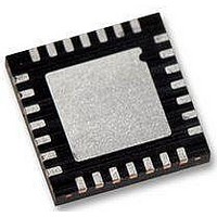
WM8986GECO/V Wolfson Microelectronics, WM8986GECO/V Datasheet - Page 6

WM8986GECO/V
Manufacturer Part Number
WM8986GECO/V
Description
Audio Amplifiers Class D Headphone DAC + Line Out
Manufacturer
Wolfson Microelectronics
Datasheet
1.WM8986GECOV.pdf
(88 pages)
Specifications of WM8986GECO/V
Product
Class-D
Output Power
40 mW
Thd Plus Noise
- 86 dB
Operating Supply Voltage
1.71 V to 3.6 V, 2.5 V to 3.6 V
Maximum Operating Temperature
+ 85 C
Mounting Style
SMD/SMT
Audio Load Resistance
16 Ohms
Minimum Operating Temperature
- 40 C
Output Signal Type
Differential
Supply Voltage (max)
3.6 V
Supply Voltage (min)
1.71 V, 2.5 V
Output Type
Differential
Package / Case
QFN-28
Lead Free Status / RoHS Status
Lead free / RoHS Compliant
PARAMETER
Digital supply range (Core)
Digital supply range (Buffer)
Analogue supply range
Ground
WM8986
ABSOLUTE MAXIMUM RATINGS
Absolute Maximum Ratings are stress ratings only. Permanent damage to the device may be caused by continuously
operating at or beyond these limits. Device functional operating limits and guaranteed performance specifications are given
under Electrical Characteristics at the test conditions specified.
Wolfson tests its package types according to IPC/JEDEC J-STD-020B for Moisture Sensitivity to determine acceptable storage
conditions prior to surface mount assembly. These levels are:
MSL1 = unlimited floor life at <30°C / 85% Relative Humidity. Not normally stored in moisture barrier bag.
MSL2 = out of bag storage for 1 year at <30°C / 60% Relative Humidity. Supplied in moisture barrier bag.
MSL3 = out of bag storage for 168 hours at <30°C / 60% Relative Humidity. Supplied in moisture barrier bag.
The Moisture Sensitivity Level for each package type is specified in Ordering Information.
DBVDD, DCVDD, AVDD1, AVDD2 supply voltages
Voltage range digital inputs
Voltage range analogue inputs
Operating Temperature Range
Storage temperature prior to soldering
Storage temperature after soldering
Notes:
1.
2.
3.
4.
RECOMMENDED OPERATING CONDITIONS
Notes:
1.
2.
w
Analogue and digital grounds must always be within 0.3V of each other.
All digital and analogue supplies are internally independent (i.e. not connected).
Analogue supply voltages AVDD1 and AVDD2 should be greater than or equal to the DCVDD digital supply voltage.
DBVDD must be greater than or equal to DCVDD.
Analogue supply voltages should not be less than digital supply voltages.
DBVDD must be greater than or equal to DCVDD.
ESD Sensitive Device. This device is manufactured on a CMOS process. It is therefore generically susceptible
to damage from excessive static voltages. Proper ESD precautions must be taken during handling and storage
of this device.
CONDITION
DGND, AGND1, AGND2
AVDD1, AVDD2
SYMBOL
DCVDD
DBVDD
CONDITIONS
TEST
AGND1 -0.3V
DGND -0.3V
-40°C
-65°C
-0.3V
1.71
1.71
2.5
MIN
MIN
1
30°C max / 85% RH max
1
TYP
0
PD, Rev 4.1, June 2009
DBVDD +0.3V
AVDD1 +0.3V
MAX
3.6
3.6
3.6
+150°C
+85°C
+4.5V
MAX
Production Data
UNIT
V
V
V
V
6


