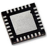
WM8986GECO/V Wolfson Microelectronics, WM8986GECO/V Datasheet - Page 63

WM8986GECO/V
Manufacturer Part Number
WM8986GECO/V
Description
Audio Amplifiers Class D Headphone DAC + Line Out
Manufacturer
Wolfson Microelectronics
Datasheet
1.WM8986GECOV.pdf
(88 pages)
Specifications of WM8986GECO/V
Product
Class-D
Output Power
40 mW
Thd Plus Noise
- 86 dB
Operating Supply Voltage
1.71 V to 3.6 V, 2.5 V to 3.6 V
Maximum Operating Temperature
+ 85 C
Mounting Style
SMD/SMT
Audio Load Resistance
16 Ohms
Minimum Operating Temperature
- 40 C
Output Signal Type
Differential
Supply Voltage (max)
3.6 V
Supply Voltage (min)
1.71 V, 2.5 V
Output Type
Differential
Package / Case
QFN-28
Lead Free Status / RoHS Status
Lead free / RoHS Compliant
Production Data
RESETTING THE CHIP
POWER SUPPLIES
w
2-WIRE SERIAL CONTROL MODE
The WM8986 supports software control via a 2-wire serial bus. Many devices can be controlled by
the same bus, and each device has a unique 7-bit device address (this is not the same as the 7-bit
address of each register in the WM8986).
The WM8986 operates as a slave device only. The controller indicates the start of data transfer with
a high to low transition on SDIN while SCLK remains high. This indicates that a device address and
data will follow. All devices on the 2-wire bus respond to the start condition and shift in the next eight
bits on SDIN (7-bit address + Read/Write bit, MSB first). If the device address received matches the
address of the WM8986, the WM8986 responds by pulling SDIN low on the next clock pulse (ACK).
If the address is not recognised or the R/W bit is ‘1’ when operating in write only mode, the WM8986
returns to the idle condition and waits for a new start condition and valid address.
During a write, once the WM8986 has acknowledged a correct address, the controller sends the first
byte of control data (B15 to B8, i.e. the WM8986 register address plus the first bit of register data).
The WM8986 then acknowledges the first data byte by driving SDIN low for one clock cycle. The
controller then sends the second byte of control data (B7 to B0, i.e. the remaining 8 bits of register
data), and the WM8986 acknowledges again by pulling SDIN low.
Transfer is complete when there is a low to high transition on SDIN while SCLK is high. After a
complete sequence the WM8986 returns to the idle state and waits for another start condition. If a
start or stop condition is detected out of sequence at any point during data transfer (i.e. SDIN
changes while SCLK is high), the control interface returns to the idle condition.
Figure 35 2-Wire Serial Control Interface
In 2-wire mode the WM8986 has a fixed device address, 0011010.
The WM8986 can be reset by performing a write of any value to the software reset register (address
0h). This will cause all register values to be reset to their default values. In addition to this there is a
Power-On Reset (POR) circuit which ensures that the registers are initially set to default when the
device is powered up.
The WM8986 requires four separate power supplies:
AVDD1 and AGND1: Analogue supply, powers all internal analogue functions and output drivers
LOUT1, ROUT1, OUT3 and OUT4. AVDD1 must be between 2.5V and 3.6V and has the most
significant impact on overall power consumption (except for power consumed in the headphones).
Higher AVDD1 will improve audio quality.
AVDD2 and AGND2: Output driver supplies, power LOUT2 and ROUT2. AVDD2 must be between
2.5V and 3.6V. AVDD2 can be tied to AVDD1, but it requires separate layout and decoupling
capacitors to curb harmonic distortion.
DCVDD: Digital core supply, powers all digital functions except the audio and control interface pads.
DCVDD must be between 1.71V and 3.6V, and has no effect on audio quality. The return path for
DCVDD is DGND, which is shared with DBVDD.
DBVDD must be between 1.71V and 3.6V. DBVDD return path is through DGND.
It is possible to use the same supply voltage for all four supplies. However, digital and analogue
supplies should be routed and decoupled separately on the PCB to keep digital switching noise out
of the analogue signal paths.
SCLK
SDIN
START
DEVICE ADDRESS
(7 BITS)
RD / WR
BIT
(LOW)
ACK
register address and
CONTROL BYTE 1
1st register data bit
(BITS 15 TO 8)
(LOW)
ACK
CONTROL BYTE 1
remaining 8 bits of
(BITS 7 TO 0)
register data
PD, Rev 4.1, June 2009
(LOW)
ACK
WM8986
STOP
63


