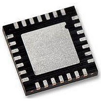
WM8986GECO/V Wolfson Microelectronics, WM8986GECO/V Datasheet - Page 14

WM8986GECO/V
Manufacturer Part Number
WM8986GECO/V
Description
Audio Amplifiers Class D Headphone DAC + Line Out
Manufacturer
Wolfson Microelectronics
Datasheet
1.WM8986GECOV.pdf
(88 pages)
Specifications of WM8986GECO/V
Product
Class-D
Output Power
40 mW
Thd Plus Noise
- 86 dB
Operating Supply Voltage
1.71 V to 3.6 V, 2.5 V to 3.6 V
Maximum Operating Temperature
+ 85 C
Mounting Style
SMD/SMT
Audio Load Resistance
16 Ohms
Minimum Operating Temperature
- 40 C
Output Signal Type
Differential
Supply Voltage (max)
3.6 V
Supply Voltage (min)
1.71 V, 2.5 V
Output Type
Differential
Package / Case
QFN-28
Lead Free Status / RoHS Status
Lead free / RoHS Compliant
- Current page: 14 of 88
- Download datasheet (2Mb)
WM8986
SIGNAL TIMING REQUIREMENTS
SYSTEM CLOCK TIMING
Figure 2 System Clock Timing Requirements
Note:
1.
AUDIO INTERFACE TIMING – MASTER MODE
w
Test Conditions
DCVDD=1.8V, DBVDD=AVDD1=AVDD2=3.3V, DGND=AGND1=AGND2=0V, T
PARAMETER
System Clock Timing Information
MCLK cycle time
MCLK duty cycle
PLL pre-scaling and PLL N and K values should be set appropriately so that SYSCLK is no greater than 12.288MHz.
MCLK
Figure 3 Digital Audio Data Timing – Master Mode (see Control Interface)
SYMBOL
T
T
MCLKDS
MCLKY
t
MCLKL
t
MCLKY
MCLK=SYSCLK (=256fs)
t
MCLK input to PLL
MCLKH
CONDITIONS
Note 1
A
= +25
81.38
60:40
MIN
20
o
C, Slave Mode
TYP
PD, Rev 4.1, June 2009
40:60
MAX
Production Data
UNIT
ns
ns
14
Related parts for WM8986GECO/V
Image
Part Number
Description
Manufacturer
Datasheet
Request
R

Part Number:
Description:
Manufacturer:
Wolfson Microelectronics
Datasheet:


