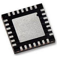
WM8986GECO/V Wolfson Microelectronics, WM8986GECO/V Datasheet - Page 19

WM8986GECO/V
Manufacturer Part Number
WM8986GECO/V
Description
Audio Amplifiers Class D Headphone DAC + Line Out
Manufacturer
Wolfson Microelectronics
Datasheet
1.WM8986GECOV.pdf
(88 pages)
Specifications of WM8986GECO/V
Product
Class-D
Output Power
40 mW
Thd Plus Noise
- 86 dB
Operating Supply Voltage
1.71 V to 3.6 V, 2.5 V to 3.6 V
Maximum Operating Temperature
+ 85 C
Mounting Style
SMD/SMT
Audio Load Resistance
16 Ohms
Minimum Operating Temperature
- 40 C
Output Signal Type
Differential
Supply Voltage (max)
3.6 V
Supply Voltage (min)
1.71 V, 2.5 V
Output Type
Differential
Package / Case
QFN-28
Lead Free Status / RoHS Status
Lead free / RoHS Compliant
Production Data
Figure 9 Typical Power up Sequence where DCVDD is Powered before AVDD1
w
Figure 9 shows a typical power-up sequence where DCVDD comes up first. First it is assumed that
DCVDD is already up to specified operating voltage. When AVDD1 goes above the minimum
threshold, V
chip is held in reset. In this condition, all writes to the control interface are ignored. When AVDD1
rises to V
control interface may take place.
On power down, where DCVDD falls first, PORB is asserted low whenever DCVDD drops below the
minimum threshold V
Table 2 Typical POR Operation (Typical Simulated Values)
Notes:
1.
2.
3.
SYMBOL
V
V
V
V
V
pora_on
pora_off
pord_on
pord_off
If AVDD1 and DCVDD suffer a brown-out (i.e. drop below the minimum recommended
operating level but do not go below V
resume normal operation when the voltage is back to the recommended level again.
The chip will enter reset at power down when AVDD1 or DCVDD falls below V
This may be important if the supply is turned on and off frequently by a power management
system.
The minimum t
specification is guaranteed by design rather than test.
pora
pora_on
pora
, there is enough voltage for the circuit to guarantee PORB is asserted low and the
, PORB is released high and all registers are in their default state and writes to the
MIN
0.4
0.9
0.4
0.5
0.4
por
pord_off
period is maintained even if DCVDD and AVDD1 have zero rise time. This
TYP
0.6
1.2
0.6
0.7
0.6
.
MAX
0.8
1.6
0.8
0.9
0.8
UNIT
V
V
V
V
V
pora_off
or V
pord_off
) then the chip will not reset and will
PD, Rev 4.1, June 2009
pora_off
WM8986
or V
pord_off
19
.


