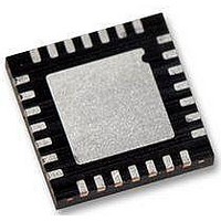
WM8986GECO/V Wolfson Microelectronics, WM8986GECO/V Datasheet - Page 74

WM8986GECO/V
Manufacturer Part Number
WM8986GECO/V
Description
Audio Amplifiers Class D Headphone DAC + Line Out
Manufacturer
Wolfson Microelectronics
Datasheet
1.WM8986GECOV.pdf
(88 pages)
Specifications of WM8986GECO/V
Product
Class-D
Output Power
40 mW
Thd Plus Noise
- 86 dB
Operating Supply Voltage
1.71 V to 3.6 V, 2.5 V to 3.6 V
Maximum Operating Temperature
+ 85 C
Mounting Style
SMD/SMT
Audio Load Resistance
16 Ohms
Minimum Operating Temperature
- 40 C
Output Signal Type
Differential
Supply Voltage (max)
3.6 V
Supply Voltage (min)
1.71 V, 2.5 V
Output Type
Differential
Package / Case
QFN-28
Lead Free Status / RoHS Status
Lead free / RoHS Compliant
WM8986
w
34 (22h)
35 (23h)
36 (24h)
37 (25h)
38 (26h)
39 (27h)
41 (29h)
42 (2Ah)
43 (2Bh)
44 (2Ch)
REGISTER
ADDRESS
8:0
8:0
8:5
4
3:0
8:6
5:0
8:0
8:0
8:4
3:0
8:3
2
1:0
8
7
8
7
6
5
BIT
PLL
PRESCALE
PLLN[3:0]
PLLK[23:18]
PLLK[17:9]
PLLK[8:0]
DEPTH3D
POBCTRL
BYPL2RMIX
BYPR2LMIX
RIN2INPPGA
LABEL
000000000
000000000
0000
0
1000
000
01100
010010011
011101001
00000
0000
0000 00
0
00
0
0
0
0
0
1
DEFAULT
Reserved
Reserved
Reserved
Divide MCLK by 2 before input to PLL
Integer (N) part of PLL input/output frequency
ratio. Use values greater than 5 and less than
13.
Reserved
Fractional (K) part of PLL1 input/output
frequency ratio (treat as one 24-digit binary
number).
Fractional (K) part of PLL1 input/output
frequency ratio (treat as one 24-digit binary
number).
Fractional (K) part of PLL1 input/output
frequency ratio (treat as one 24-digit binary
number).
Reserved
Stereo depth
0000: 0% (minimum 3D effect)
0001: 6.67%
....
1110: 93.3%
1111: 100% (maximum 3D effect)
Reserved
VMID independent current bias control
0 = Disable VMID independent current bias
1 = Enable VMID independent current bias
Reserved
Left channel input PGA stage to right output
mixer
0 = not selected
1 = selected
Right channel input PGA stage to Left output
mixer
0 = not selected
1 = selected
Reserved
Reserved
Reserved
Connect RIN pin to right channel input PGA
negative terminal.
0=RIN not connected to input PGA
1=RIN connected to right channel input PGA
amplifier negative terminal.
DESCRIPTION
PD, Rev 4.1, June 2009
Master Clock
and Phase
Locked Loop
(PLL)
Master Clock
and Phase
Locked Loop
(PLL)
Master Clock
and Phase
Locked Loop
(PLL)
Master Clock
and Phase
Locked Loop
(PLL)
Master Clock
and Phase
Locked Loop
(PLL)
3D Stereo
Enhancement
Analogue
Outputs
Analogue
Outputs
Analogue
Outputs
Input Signal
Path
Production Data
REFER TO
74


