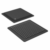
ADSP-21062LABZ-160 Analog Devices Inc, ADSP-21062LABZ-160 Datasheet - Page 11

ADSP-21062LABZ-160
Manufacturer Part Number
ADSP-21062LABZ-160
Description
IC,DSP,32-BIT,CMOS,BGA,225PIN,PLASTIC
Manufacturer
Analog Devices Inc
Series
SHARC®r
Type
Floating Pointr
Specifications of ADSP-21062LABZ-160
Interface
Host Interface, Link Port, Serial Port
Clock Rate
40MHz
Non-volatile Memory
External
On-chip Ram
256kB
Voltage - I/o
3.30V
Voltage - Core
3.30V
Operating Temperature
-40°C ~ 85°C
Mounting Type
Surface Mount
Package / Case
225-BGA
Package
225BGA
Numeric And Arithmetic Format
Floating-Point
Maximum Speed
40 MHz
Ram Size
256 KB
Device Million Instructions Per Second
40 MIPS
Lead Free Status / RoHS Status
Lead free / RoHS Compliant
Available stocks
Company
Part Number
Manufacturer
Quantity
Price
Company:
Part Number:
ADSP-21062LABZ-160
Manufacturer:
SAMSUNG
Quantity:
591
Company:
Part Number:
ADSP-21062LABZ-160
Manufacturer:
Analog Devices Inc
Quantity:
10 000
ADSP-21060/ADSP-21060L/ADSP-21062/ADSP-21062L/ADSP-21060C/ADSP-21060LC
Table 3. Pin Descriptions (Continued)
Pin
ACK
SBTS
IRQ2–0
FLAG3–0
TIMEXP
HBR
HBG
CS
REDY
DMAR2–1
DMAG2–1
BR6–1
ID2–0
RPBA
CPA
DTx
DRx
TCLKx
RCLKx
A = Asynchronous, G = Ground, I = Input, O = Output, P = Power Supply, S = Synchronous, (A/D) = Active Drive, (O/D) = Open Drain,
T = Three-State (when SBTS is asserted, or when the ADSP-2106x is a bus slave)
Type
I/O/S
I/S
I/A
I/O/A
O
I/A
I/O
I/A
O (O/D)
I/A
O/T
I/O/S
O (O/D)
I/S
I/O (O/D)
O
I
I/O
I/O
Function
Memory Acknowledge. External devices can deassert ACK (low) to add wait states to an external memory
access. ACK is used by I/O devices, memory controllers, or other peripherals to hold off completion of an
external memory access. The ADSP-2106x deasserts ACK as an output to add waitstates to a synchronous
access of its internal memory. In a multiprocessing system, a slave ADSP-2106x deasserts the bus master’s
ACK input to add wait state(s) to an access of its internal memory. The bus master has a keeper latch on its
ACK pin that maintains the input at the level to which it was last driven.
Suspend Bus Three-State. External devices can assert SBTS (low) to place the external bus address, data,
selects, and strobes in a high impedance state for the following cycle. If the ADSP-2106x attempts to access
external memory while SBTS is asserted, the processor will halt and the memory access will not be completed
until SBTS is deasserted. SBTS should only be used to recover from host processor/ADSP-2106x deadlock,
or used with a DRAM controller.
Interrupt Request Lines. May be either edge-triggered or level-sensitive.
Flag Pins. Each is configured via control bits as either an input or output. As an input, they can be tested as
a condition. As an output, they can be used to signal external peripherals.
Timer Expired. Asserted for four cycles when the timer is enabled and TCOUNT decrements to zero.
Host Bus Request. This pin must be asserted by a host processor to request control of the ADSP-2106x’s
external bus. When HBR is asserted in a multiprocessing system, the ADSP-2106x that is bus master will
relinquish the bus and assert HBG. To relinquish the bus, the ADSP-2106x places the address, data, select
and strobe lines in a high impedance state. HBR has priority over all ADSP-2106x bus requests BR6–1 in a
multiprocessing system.
Host Bus Grant. Acknowledges a bus request, indicating that the host processor may take control of the
external bus. HBG is asserted (held low) by the ADSP-2106x until HBR is released. In a multiprocessing system,
HBG is output by the ADSP-2106x bus master and is monitored by all others.
Chip Select. Asserted by host processor to select the ADSP-2106x.
Host Bus Acknowledge. The ADSP-2106x deasserts REDY (low) to add wait states to an asynchronous access
of its internal memory or IOP registers by a host. This pin is an open-drain output (O/D) by default; it can be
programmed in the ADREDY bit of the SYSCON register to be active drive (A/D). REDY will only be output if
the CS and HBR inputs are asserted.
DMA Request 1 (DMA Channel 7) and DMA Request 2 (DMA Channel 8).
DMA Grant 1 (DMA Channel 7) and DMA Grant 2 (DMA Channel 8).
Multiprocessing Bus Requests. Used by multiprocessing ADSP-2106xs to arbitrate for bus master-ship. An
ADSP-2106x only drives its own BRx line (corresponding to the value of its ID2-0 inputs) and monitors all
others. In a multiprocessor system with less than six ADSP-2106xs, the unused BRx pins should be pulled
high; the processor’s own BRx line must not be pulled high or low because it is an output.
Multiprocessing ID. Determines which multiprocessing bus request (BR1– BR6) is used by ADSP-2106x.
ID = 001 corresponds to BR1, ID = 010 corresponds to BR2, etc. ID = 000 in single-processor systems. These
lines are a system configuration selection that should be hardwired or changed at reset only.
Rotating Priority Bus Arbitration Select. When RPBA is high, rotating priority for multiprocessor bus
arbitration is selected. When RPBA is low, fixed priority is selected. This signal is a system configuration
selection that must be set to the same value on every ADSP-2106x. If the value of RPBA is changed during
system operation, it must be changed in the same CLKIN cycle on every ADSP-2106x.
Core Priority Access. Asserting its CPA pin allows the core processor of an ADSP-2106x bus slave to interrupt
background DMA transfers and gain access to the external bus. CPA is an open drain output that is connected
to all ADSP-2106xs in the system. The CPA pin has an internal 5 k: pull-up resistor. If core access priority is
not required in a system, the CPA pin should be left unconnected.
Data Transmit (Serial Ports 0, 1). Each DT pin has a 50 k: internal pull-up resistor.
Data Receive (Serial Ports 0, 1). Each DR pin has a 50 k: internal pull-up resistor.
Transmit Clock (Serial Ports 0, 1). Each TCLK pin has a 50 k: internal pull-up resistor.
Receive Clock (Serial Ports 0, 1). Each RCLK pin has a 50 k: internal pull-up resistor.
Rev. F | Page 11 of 64 | March 2008


