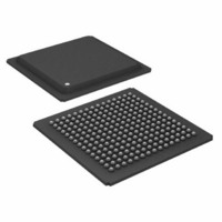
ADSP-21062LABZ-160 Analog Devices Inc, ADSP-21062LABZ-160 Datasheet - Page 20

ADSP-21062LABZ-160
Manufacturer Part Number
ADSP-21062LABZ-160
Description
IC,DSP,32-BIT,CMOS,BGA,225PIN,PLASTIC
Manufacturer
Analog Devices Inc
Series
SHARC®r
Type
Floating Pointr
Specifications of ADSP-21062LABZ-160
Interface
Host Interface, Link Port, Serial Port
Clock Rate
40MHz
Non-volatile Memory
External
On-chip Ram
256kB
Voltage - I/o
3.30V
Voltage - Core
3.30V
Operating Temperature
-40°C ~ 85°C
Mounting Type
Surface Mount
Package / Case
225-BGA
Package
225BGA
Numeric And Arithmetic Format
Floating-Point
Maximum Speed
40 MHz
Ram Size
256 KB
Device Million Instructions Per Second
40 MIPS
Lead Free Status / RoHS Status
Lead free / RoHS Compliant
Available stocks
Company
Part Number
Manufacturer
Quantity
Price
Company:
Part Number:
ADSP-21062LABZ-160
Manufacturer:
SAMSUNG
Quantity:
591
Company:
Part Number:
ADSP-21062LABZ-160
Manufacturer:
Analog Devices Inc
Quantity:
10 000
ADSP-21060/ADSP-21060L/ADSP-21062/ADSP-21062L/ADSP-21060C/ADSP-21060LC
EXTERNAL POWER DISSIPATION (3.3 V)
Total power dissipation has two components, one due to inter-
nal circuitry and one due to the switching of external output
drivers. Internal power dissipation is dependent on the instruc-
tion execution sequence and the data operands involved.
Internal power dissipation is calculated in the following way:
The external component of total power dissipation is caused by
the switching of output pins. Its magnitude depends on:
and is calculated by:
The load capacitance should include the processor’s package
capacitance (CIN). The switching frequency includes driving
the load high and then back low. Address and data pins can
Table 6. External Power Calculations (3.3 V Devices)
ABSOLUTE MAXIMUM RATINGS
Stresses greater than those listed
damage to the device. These are stress ratings only; functional
operation of the device at these or any other conditions greater
Table 7. Absolute Maximum Ratings
Pin Type
Address
MS0
WR
Data
ADDRCLK
Parameter
Supply Voltage (V
Input Voltage
Output Voltage Swing
Load Capacitance
Storage Temperature Range
Lead Temperature (5 seconds)
Junction Temperature Under Bias
• the number of output pins that switch during each cycle
• the maximum frequency at which they can switch (f)
• their load capacitance (C)
• their voltage swing (V
P
P
INT
(O)
EXT
= I
= O u C u V
DDIN
u V
DD
DD
DD
)
2
u f
DD
)
No. of Pins
15
1
1
32
1
Table 7
may cause permanent
% Switching
50
0
–
50
–
Rev. F | Page 20 of 64 | March 2008
u C
u 44.7 pF
u 44.7 pF
u 44.7 pF
u 14.7 pF
u 4.7 pF
ADSP-21060/ADSP-21060C
ADSP-21062
5 V
–0.3 V to +7.0 V
–0.5 V to V
–65qC to +150qC
130qC
–0.5 V to V
200 pF
280qC
drive high and low at a maximum rate of 1/(2t
strobe can switch every cycle at a frequency of 1/t
switch at 1/(2t
Example: Estimate P
The P
drive:
A typical power consumption can now be calculated for these
conditions by adding a typical internal power dissipation:
Note that the conditions causing a worst-case P
from those causing a worst-case P
occur while 100% of the output pins are switching from all ones
to all zeros. Note also that it is not common for an application to
have 100% or even 50% of the outputs switching
simultaneously.
than those indicated in the operational sections of this specifica-
tion is not implied. Exposure to absolute maximum rating
conditions for extended periods may affect device reliability.
• A system with one bank of external data memory RAM
• Four 128K u 8 RAM chips are used, each with a load of
• External data memory writes occur every other cycle, a rate
• The instruction cycle rate is 40 MHz (t
P
(32-bit)
10 pF
of 1/(4t
TOTAL
EXT
equation is calculated for each class of pins that can
= P
DD
DD
u f
u 10 MHz
u 10 MHz
u 20 MHz
u 10 MHz
u 20 MHz
CK
+ 0.5 V
+ 0.5 V
EXT
), with 50% of the pins switching
CK
), but selects can switch on each cycle.
+ (I
DDIN
EXT
with the following assumptions:
2
u 5.0 V)
u V
u 10.9 V
u 10.9 V
u 10.9 V
u 10.9 V
u 10.9 V
ADSP-21060L/ADSP-21060LC
ADSP-21062L
3.3 V
–0.3 V to +4.6 V
–0.5 V to V
–0.5 V to V
200 pF
–65qC to +150qC
280qC
130qC
DD
INT
2
. Maximum P
DD
DD
CK
= P
= 0.037 W
= 0.000 W
= 0.010 W
= 0.026 W
= 0.001 W
+0.5 V
+ 0.5 V
= 25 ns)
CK
EXT
EXT
). The write
P
CK
INT
EXT
are different
. Select pins
cannot
= 0.074 W


