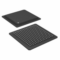
ADSP-21062LABZ-160 Analog Devices Inc, ADSP-21062LABZ-160 Datasheet - Page 47

ADSP-21062LABZ-160
Manufacturer Part Number
ADSP-21062LABZ-160
Description
IC,DSP,32-BIT,CMOS,BGA,225PIN,PLASTIC
Manufacturer
Analog Devices Inc
Series
SHARC®r
Type
Floating Pointr
Specifications of ADSP-21062LABZ-160
Interface
Host Interface, Link Port, Serial Port
Clock Rate
40MHz
Non-volatile Memory
External
On-chip Ram
256kB
Voltage - I/o
3.30V
Voltage - Core
3.30V
Operating Temperature
-40°C ~ 85°C
Mounting Type
Surface Mount
Package / Case
225-BGA
Package
225BGA
Numeric And Arithmetic Format
Floating-Point
Maximum Speed
40 MHz
Ram Size
256 KB
Device Million Instructions Per Second
40 MIPS
Lead Free Status / RoHS Status
Lead free / RoHS Compliant
Available stocks
Company
Part Number
Manufacturer
Quantity
Price
Company:
Part Number:
ADSP-21062LABZ-160
Manufacturer:
SAMSUNG
Quantity:
591
Company:
Part Number:
ADSP-21062LABZ-160
Manufacturer:
Analog Devices Inc
Quantity:
10 000
ADSP-21060/ADSP-21060L/ADSP-21062/ADSP-21062L/ADSP-21060C/ADSP-21060LC
TEST CONDITIONS
For the ac signal specifications (timing parameters), see
Specifications on Page
disable time, output enable time, and capacitive loading. The
timing specifications for the DSP apply for the voltage reference
levels in
Output Disable Time
Output pins are considered to be disabled when they stop driv-
ing, go into a high impedance state, and start to decay from their
output high or low voltage. The time for the voltage on the bus
to decay by 'V is dependent on the capacitive load, C
load current, I
lowing equation:
The output disable time t
t
the interval from when the reference signal switches to when the
output voltage decays 'V from the measured output high or
output low voltage. t
and with 'V equal to 0.5 V.
Output Enable Time
Output pins are considered to be enabled when they have made
a transition from a high impedance state to when they start driv-
ing. The output enable time t
reference signal reaches a high or low voltage level to when the
MEASURED
Figure 28. Voltage Reference Levels for AC Measurements (Except Output
REFERENCE
V
V
OH (MEASURED)
OL (MEASURED)
SIGNAL
OUTPUT
Figure
and t
INPUT
OR
t
DIS
DECAY
L
OUTPUT STOPS
. This decay time can be approximated by the fol-
28.
DRIVING
Figure 29. Output Enable/Disable
as shown in
DECAY
1.5V
t
MEASURED
V
V
21. These specifications include output
OH (MEASURED)
OL (MEASURED)
t
P
DECAY
DIS
Enable/Disable)
is calculated with test loads C
EXT
is the difference between
HIGH IMPEDANCE STATE.
TEST CONDITIONS CAUSE
THIS VOLTAGE TO BE
APPROXIMATELY 1.5V
ENA
=
Figure
is the interval from when a
C
------------- -
+ V
- V
L
I
'
L
V
29. The time t
OUTPUT STARTS
1.5V
t
ENA
1.0V
2.0V
DRIVING
V
V
OH (MEASURED)
OL (MEASURED)
Rev. F | Page 47 of 64 | March 2008
MEASURED
L
, and the
L
Timing
and I
is
L
,
output has reached a specified high or low trip point, as shown
in the Output Enable/Disable diagram
pins (such as the data bus) are enabled, the measurement value
is that of the first pin to start driving.
Example System Hold Time Calculation
To determine the data output hold time in a particular system,
first calculate t
to be the difference between the ADSP-2106x’s output voltage
and the input threshold for the device requiring the hold time. A
typical 'V will be 0.4 V. C
line), and I
line). The hold time will be t
time (i.e., t
Capacitive Loading
Output delays and holds are based on standard capacitive loads:
50 pF on all pins (see
tions given should be derated by a factor of 1.5 ns/50 pF for
loads other than the nominal value of 50 pF.
Figure
varies with capacitance.
graphically how output delays and holds vary with load capaci-
tance. (Note that this graph or derating does not apply to output
disable delays; see the previous section Output Disable Time
under Test Conditions.) The graphs of
Figure
shown.
Output Drive Characteristics
Figure 31
ers of the ADSP-2106x. The curves represent the current drive
capability of the output drivers as a function of output voltage.
Figure 30. Equivalent Device Loading for AC Measurements (Includes All
OUTPUT
33,
37, and
shows typical I-V characteristics for the output driv-
PIN
Figure
DATRWH
TO
L
is the total leakage or three-state current (per data
DECAY
Figure 38
50pF
for the write cycle).
37, and
using the equation given above. Choose 'V
Figure
Figure 34
may not be linear outside the ranges
Figure 38
L
is the total bus capacitance (per data
Fixtures)
DECAY
30). The delay and hold specifica-
I
I
OH
OL
plus the minimum disable
and
show how output rise time
Figure 36
(Figure
Figure
+1.5V
Figure
32,
29). If multiple
show
Figure
32,
33,


