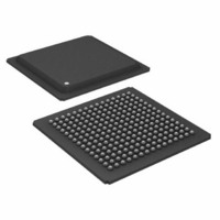
ADSP-21062LABZ-160 Analog Devices Inc, ADSP-21062LABZ-160 Datasheet - Page 39

ADSP-21062LABZ-160
Manufacturer Part Number
ADSP-21062LABZ-160
Description
IC,DSP,32-BIT,CMOS,BGA,225PIN,PLASTIC
Manufacturer
Analog Devices Inc
Series
SHARC®r
Type
Floating Pointr
Specifications of ADSP-21062LABZ-160
Interface
Host Interface, Link Port, Serial Port
Clock Rate
40MHz
Non-volatile Memory
External
On-chip Ram
256kB
Voltage - I/o
3.30V
Voltage - Core
3.30V
Operating Temperature
-40°C ~ 85°C
Mounting Type
Surface Mount
Package / Case
225-BGA
Package
225BGA
Numeric And Arithmetic Format
Floating-Point
Maximum Speed
40 MHz
Ram Size
256 KB
Device Million Instructions Per Second
40 MIPS
Lead Free Status / RoHS Status
Lead free / RoHS Compliant
Available stocks
Company
Part Number
Manufacturer
Quantity
Price
Company:
Part Number:
ADSP-21062LABZ-160
Manufacturer:
SAMSUNG
Quantity:
591
Company:
Part Number:
ADSP-21062LABZ-160
Manufacturer:
Analog Devices Inc
Quantity:
10 000
ADSP-21060/ADSP-21060L/ADSP-21062/ADSP-21062L/ADSP-21060C/ADSP-21060LC
Table 25. Link Port Service Request Interrupts:1u and 2u Speed Operations
1
Link Ports —2 × CLK Speed Operation
Calculation of link receiver data setup and hold relative to link
clock is required to determine the maximum allowable skew
that can be introduced in the transmission path between
LDATA and LCLK. Setup skew is the maximum delay that can
be introduced in LDATA relative to LCLK:
Table 26. Link Ports—Receive
1
2
3
4
Parameter
Timing Requirements
t
t
Only required for interrupt recognition in the current cycle.
Parameter
Timing Requirements
t
t
t
t
t
Switching Characteristics
t
t
For ADSP-21060L, specification is 5 ns min.
For ADSP-21062, specification is 4 ns min, for ADSP-21060LC, specification is 4.5 ns min.
LACK goes low with t
For ADSP-21060L, specification is 6 ns min, 18 ns max. For ADSP-21060C, specification is 6 ns min, 16.5 ns max. For ADSP-21060LC, specification is 6 ns min, 18.5 ns max.
SLCK
HLCK
SLDCL
HLDCL
LCLKIW
LCLKRWL
LCLKRWH
DLAHC
DLALC
Setup Skew = t
Data Setup Before LCLK Low
Data Hold After LCLK Low
LCLK Period (2u Operation)
LCLK Width Low
LCLK Width High
LACK High Delay After CLKIN High
LACK Low Delay After LCLK High
LCLKTWH
DLALC
LACK/LCLK Setup Before CLKIN Low
LACK/LCLK Hold After CLKIN Low
relative to rise of LCLK after first nibble, but does not go low if the receiver’s link buffer is not about to fill.
min – t
1
2
DLDCH
– t
SLDCL
4
3
Rev. F | Page 39 of 64 | March 2008
1
1
Min
10
2
Min
2.5
t
4.5
4.25
18 + DT/2
6
2.25
CK
/2
Hold skew is the maximum delay that can be introduced in
LCLK relative to LDATA:
Calculations made directly from 2 speed specifications will
result in unrealistically small skew times because they include
multiple tester guardbands.
Note that link port transfers at 2× CLK speed at 40 MHz
(t
fers at 33 MHz (t
5 V
CK
Max
Hold Skew = t
5 V
= 25 ns) may fail. However, 2× CLK speed link port trans-
Max
28.5 + DT/2
16
CK
LCLKTWL
= 30 ns) work as specified.
Min
10
2
Min
2.25
2.25
t
5.25
4
18 + DT/2
6
CK
/2
min – t
HLDCH
3.3 V
3.3 V
Max
Max
29.5 + DT/2
16
– t
HLDCL
Unit
ns
ns
ns
ns
ns
ns
ns
Unit
ns
ns


