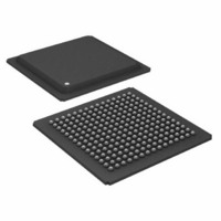
ADSP-21062LABZ-160 Analog Devices Inc, ADSP-21062LABZ-160 Datasheet - Page 29

ADSP-21062LABZ-160
Manufacturer Part Number
ADSP-21062LABZ-160
Description
IC,DSP,32-BIT,CMOS,BGA,225PIN,PLASTIC
Manufacturer
Analog Devices Inc
Series
SHARC®r
Type
Floating Pointr
Specifications of ADSP-21062LABZ-160
Interface
Host Interface, Link Port, Serial Port
Clock Rate
40MHz
Non-volatile Memory
External
On-chip Ram
256kB
Voltage - I/o
3.30V
Voltage - Core
3.30V
Operating Temperature
-40°C ~ 85°C
Mounting Type
Surface Mount
Package / Case
225-BGA
Package
225BGA
Numeric And Arithmetic Format
Floating-Point
Maximum Speed
40 MHz
Ram Size
256 KB
Device Million Instructions Per Second
40 MIPS
Lead Free Status / RoHS Status
Lead free / RoHS Compliant
Available stocks
Company
Part Number
Manufacturer
Quantity
Price
Company:
Part Number:
ADSP-21062LABZ-160
Manufacturer:
SAMSUNG
Quantity:
591
Company:
Part Number:
ADSP-21062LABZ-160
Manufacturer:
Analog Devices Inc
Quantity:
10 000
ADSP-21060/ADSP-21060L/ADSP-21062/ADSP-21062L/ADSP-21060C/ADSP-21060LC
Synchronous Read/Write—Bus Slave
Use these specifications for bus master accesses of a slave’s IOP
registers or internal memory (in multiprocessor memory space).
The bus master must meet the bus slave timing requirements.
Table 17. Synchronous Read/Write—Bus Slave
1
2
3
4
5
Parameter
Timing Requirements
t
t
t
t
t
t
t
Switching Characteristics
t
t
t
t
t
For ADSP-21060C specification is –3.5 – 5DT/16 ns min, 8 + 7DT/16 ns max; for ADSP-21060LC specification is –3.75 – 5DT/16 ns min, 8 + 7DT/16 ns max.
For ADSP-21062/ADSP-21062L/ADSP-21060C specification is 19 + 5DT/16 ns max; for ADSP-21060LC specification is 19.25 + 5DT/16 ns max.
See
t
SRWLI
DACKAD
SADRI
HADRI
SRWLI
HRWLI
RWHPI
SDATWH
HDATWH
SDDATO
DATTR
DACKAD
ACKTR
greater than 19 + 3DT/4, then ACK is valid 14 + DT/4 (max) after CLKIN. A slave that sees an address with an M field match will respond with ACK regardless of the state
of MMSWS or strobes. A slave will three-state ACK every cycle with t
WRITE ACCESS
READ ACCESS
Example System Hold Time Calculation on Page 47
(min) = 9.5 + 5DT/16 when Multiprocessor Memory Space Wait State (MMSWS bit in WAIT register) is disabled; when MMSWS is enabled, t
is true only if the address and SW inputs have setup times (before CLKIN) greater than 10 + DT/8 and less than 19 + 3DT/4. If the address and inputs have setup times
ADDRESS
CLKIN
DATA
DATA
(OU T)
(IN)
ACK
W R
RD
Address, SW Setup Before CLKIN
Address, SW Hold After CLKIN
RD/WR Low Setup Before CLKIN
RD/WR Low Hold After CLKIN
RD/WR Pulse High
Data Setup Before WR High
Data Hold After WR High
Data Delay After CLKIN
Data Disable After CLKIN
ACK Delay After Address, SW
ACK Disable After CLKIN
3
5
4
t
SD D AT O
for calculation of hold times given capacitive and dc loads.
Figure 17. Synchronous Read/Write—Bus Slave
5
2
1
Rev. F | Page 29 of 64 | March 2008
ACKTR
t
D AC K AD
.
t
S A DR I
t
t
SR W LI
SR WLI
Min
15 + DT/2
9.5 + 5DT/16
–4 – 5DT/16
3
5
1
0 – DT/8
–1 – DT/8
t
S D AT WH
t
H RW L I
t
t
H RW L I
5 V and 3.3 V
H A DR I
t
D AT T R
t
AC K TR
Max
5 + DT/2
8 + 7DT/16
18 + 5DT/16
7 – DT/8
9
6 – DT/8
t
H D ATW H
t
R WH PI
t
SRWLI
R W HP I
(min)= 4 + DT/8.
Unit
ns
ns
ns
ns
ns
ns
ns
ns
ns
ns
ns


