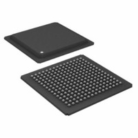
ADSP-21062LABZ-160 Analog Devices Inc, ADSP-21062LABZ-160 Datasheet - Page 13

ADSP-21062LABZ-160
Manufacturer Part Number
ADSP-21062LABZ-160
Description
IC,DSP,32-BIT,CMOS,BGA,225PIN,PLASTIC
Manufacturer
Analog Devices Inc
Series
SHARC®r
Type
Floating Pointr
Specifications of ADSP-21062LABZ-160
Interface
Host Interface, Link Port, Serial Port
Clock Rate
40MHz
Non-volatile Memory
External
On-chip Ram
256kB
Voltage - I/o
3.30V
Voltage - Core
3.30V
Operating Temperature
-40°C ~ 85°C
Mounting Type
Surface Mount
Package / Case
225-BGA
Package
225BGA
Numeric And Arithmetic Format
Floating-Point
Maximum Speed
40 MHz
Ram Size
256 KB
Device Million Instructions Per Second
40 MIPS
Lead Free Status / RoHS Status
Lead free / RoHS Compliant
Available stocks
Company
Part Number
Manufacturer
Quantity
Price
Company:
Part Number:
ADSP-21062LABZ-160
Manufacturer:
SAMSUNG
Quantity:
591
Company:
Part Number:
ADSP-21062LABZ-160
Manufacturer:
Analog Devices Inc
Quantity:
10 000
ADSP-21060/ADSP-21060L/ADSP-21062/ADSP-21062L/ADSP-21060C/ADSP-21060LC
TARGET BOARD CONNECTOR FOR EZ-ICE PROBE
The ADSP-2106x EZ-ICE
1149.1JTAG test access port of the ADSP-2106x to monitor and
control the target board processor during emulation. The
EZ-ICE probe requires the ADSP-2106x’s CLKIN, TMS, TCK,
TRST, TDI, TDO, EMU, and GND signals be made accessible
on the target system via a 14-pin connector (a 2-row 7-pin strip
header) such as that shown in Figure 5. The EZ-ICE probe plugs
directly onto this connector for chip-on-board emulation. You
must add this connector to your target board design if you
intend to use the ADSP-2106x EZ-ICE. The total trace length
between the EZ-ICE connector and the furthest device sharing
the EZ-ICE JTAG pin should be limited to 15 inches maximum
for guaranteed operation. This length restriction must include
EZ-ICE JTAG signals that are routed to one or more
ADSP-2106x devices, or a combination of ADSP-2106x devices
and other JTAG devices on the chain.
The 14-pin, 2-row pin strip header is keyed at the Pin 3 loca-
tion—Pin 3 must be removed from the header. The pins must be
0.025 inch square and at least 0.20 inch in length. Pin spacing
should be 0.1 u 0.1 inches. Pin strip headers are available from
vendors such as 3M, McKenzie, and Samtec. The BTMS, BTCK,
BTRST, and BTDI signals are provided so that the test access
port can also be used for board-level testing.
When the connector is not being used for emulation, place
jumpers between the Bxxx pins and the xxx pins as shown in
Figure
board testing, tie BTRST to GND and tie or pull up BTCK to
V
up (through BTRST on the connector) or held low for proper
operation of the ADSP-2106x. None of the Bxxx pins (Pins 5, 7,
9, and 11) are connected on the EZ-ICE probe.
DD
Figure 5. Target Board Connector for ADSP-2106x EZ-ICE Emulator
. The TRST pin must be asserted (pulsed low) after power-
5. If you are not going to use the test access port for
KEY (NO PIN)
BTRST
BTMS
BTCK
GND
BTDI
GND
11
13
(Jumpers in Place)
1
3
5
7
9
TOP VIEW
®
9
Emulator uses the IEEE
14
10
12
2
4
6
8
EMU
GND
TMS
TCK
TRST
TDI
TDO
Rev. F | Page 13 of 64 | March 2008
The JTAG signals are terminated on the EZ-ICE probe as shown
in
Table 4. Core Instruction Rate/CLKIN Ratio Selection
1
Figure 6
contain multiple ADSP-2106x processors.
Connecting CLKIN to Pin 4 of the EZ-ICE header is optional.
The emulator only uses CLKIN when directed to perform oper-
ations such as starting, stopping, and single-stepping multiple
ADSP-2106xs in a synchronous manner. If you do not need
these operations to occur synchronously on the multiple proces-
sors, simply tie Pin 4 of the EZ-ICE header to ground.
If synchronous multiprocessor operations are needed and
CLKIN is connected, clock skew between the multiple
ADSP-2106x processors and the CLKIN pin on the EZ-ICE
header must be minimal. If the skew is too large, synchronous
operations may be off by one or more cycles between proces-
sors. For synchronous multiprocessor operation TCK, TMS,
CLKIN, and EMU should be treated as critical signals in terms
of skew, and should be laid out as short as possible on your
board. If TCK, TMS, and CLKIN are driving a large number of
ADSP-2106xs (more than eight) in your system, then treat them
as a “clock tree” using multiple drivers to minimize skew. (See
Figure 7
the “High Frequency Design Considerations” section of the
ADSP-2106x User’s Manual, Revision 2.1.)
If synchronous multiprocessor operations are not needed (i.e.,
CLKIN is not connected), just use appropriate parallel termina-
tion on TCK and TMS. TDI, TDO, EMU and TRST are not
critical signals in terms of skew.
For complete information on the SHARC EZ-ICE, see the
ADSP-21000 Family JTAG EZ-ICE User's Guide and Reference.
Signal
TMS
TCK
TRST
TDI
TDO
CLKIN
EMU
TRST is driven low until the EZ-ICE probe is turned on by the emulator at software
start-up. After software start-up, is driven high.
Table
1
4.
shows JTAG scan path connections for systems that
and “JTAG Clock Tree” and “Clock Distribution” in
Termination
Driven Through 22 : Resistor (16 mA Driver)
Driven at 10 MHz Through 22 : Resistor (16 mA
Driver)
Active Low Driven Through 22 : Resistor (16 mA
Driver) (Pulled-Up by On-Chip 20 k: Resistor)
Driven by 22 : Resistor (16 mA Driver)
One TTL Load, Split Termination (160/220)
One TTL Load, Split Termination (160/220)
Active Low 4.7 k: Pull-Up Resistor, One TTL Load
(Open-Drain Output from the DSP)


