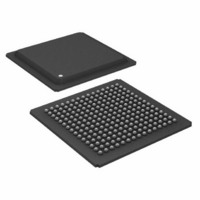
ADSP-21062LABZ-160 Analog Devices Inc, ADSP-21062LABZ-160 Datasheet - Page 24

ADSP-21062LABZ-160
Manufacturer Part Number
ADSP-21062LABZ-160
Description
IC,DSP,32-BIT,CMOS,BGA,225PIN,PLASTIC
Manufacturer
Analog Devices Inc
Series
SHARC®r
Type
Floating Pointr
Specifications of ADSP-21062LABZ-160
Interface
Host Interface, Link Port, Serial Port
Clock Rate
40MHz
Non-volatile Memory
External
On-chip Ram
256kB
Voltage - I/o
3.30V
Voltage - Core
3.30V
Operating Temperature
-40°C ~ 85°C
Mounting Type
Surface Mount
Package / Case
225-BGA
Package
225BGA
Numeric And Arithmetic Format
Floating-Point
Maximum Speed
40 MHz
Ram Size
256 KB
Device Million Instructions Per Second
40 MIPS
Lead Free Status / RoHS Status
Lead free / RoHS Compliant
Available stocks
Company
Part Number
Manufacturer
Quantity
Price
Company:
Part Number:
ADSP-21062LABZ-160
Manufacturer:
SAMSUNG
Quantity:
591
Company:
Part Number:
ADSP-21062LABZ-160
Manufacturer:
Analog Devices Inc
Quantity:
10 000
ADSP-21060/ADSP-21060L/ADSP-21062/ADSP-21062L/ADSP-21060C/ADSP-21060LC
Flags
Table 13. Flags
1
Parameter
Timing Requirements
t
t
t
t
Switching Characteristics
t
t
t
t
Flag inputs meeting these setup and hold times for instruction cycle N will affect conditional instructions in instruction cycle N+2.
SFI
HFI
DWRFI
HFIWR
DFO
HFO
DFOE
DFOD
FLAG3–0 OUT
FLAG3–0 IN
RD/WR
CLKIN
CLKIN
FLAG3–0 IN Setup Before CLKIN High
FLAG3–0 IN Hold After CLKIN High
FLAG3–0 IN Delay After RD/WR Low
FLAG3–0 IN Hold After RD/WR Deasserted
FLAG3–0 OUT Delay After CLKIN High
FLAG3–0 OUT Hold After CLKIN High
CLKIN High to FLAG3–0 OUT Enable
CLKIN High to FLAG3–0 OUT Disable
t
DWRFI
t
DFOE
FLAG INPUT
t
SFI
Rev. F | Page 24 of 64 | March 2008
1
t
1
DFO
1
Figure 13. Flags
t
t
HFI
HFIWR
1
FLAG OUTPUT
t
HFO
t
DFO
Min
8 + 5DT/16
0 – 5DT/16
0
4
3
5 V and 3.3 V
t
DFOD
Max
5 + 7DT/16
16
14
Unit
ns
ns
ns
ns
ns
ns
ns
ns


