ADSP-21062LABZ-160 Analog Devices Inc, ADSP-21062LABZ-160 Datasheet - Page 21
ADSP-21062LABZ-160
Manufacturer Part Number
ADSP-21062LABZ-160
Description
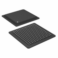
IC,DSP,32-BIT,CMOS,BGA,225PIN,PLASTIC
Manufacturer
Analog Devices Inc
Series
SHARC®r
Type
Floating Pointr
Specifications of ADSP-21062LABZ-160
Interface
Host Interface, Link Port, Serial Port
Clock Rate
40MHz
Non-volatile Memory
External
On-chip Ram
256kB
Voltage - I/o
3.30V
Voltage - Core
3.30V
Operating Temperature
-40°C ~ 85°C
Mounting Type
Surface Mount
Package / Case
225-BGA
Package
225BGA
Numeric And Arithmetic Format
Floating-Point
Maximum Speed
40 MHz
Ram Size
256 KB
Device Million Instructions Per Second
40 MIPS
Lead Free Status / RoHS Status
Lead free / RoHS Compliant
Available stocks
Company
Part Number
Manufacturer
Quantity
Price
Company:

Part Number:
ADSP-21062LABZ-160
Manufacturer:
SAMSUNG
Quantity:
591
Company:
Part Number:
ADSP-21062LABZ-160
Manufacturer:
Analog Devices Inc
Quantity:
10 000


ADSP-21060/ADSP-21060L/ADSP-21062/ADSP-21062L/ADSP-21060C/ADSP-21060LC
ESD CAUTION
PACKAGE MARKING INFORMATION
Figure 8
within the package marking for the ADSP-2106x processors
(actual marking format may vary). For a complete listing of
product availability, see
Table 8. Package Brand Information
Brand Key
t
pp
Z
ccc
vvvvvv.x
n.n
yyww
and
Table 8
ESD (electrostatic discharge) sensitive device.
Charged devices and circuit boards can discharge
without detection. Although this product features
patented or proprietary protection circuitry, damage
may occur on devices subjected to high energy ESD.
Therefore, proper ESD precautions should be taken to
avoid performance degradation or loss of functionality.
Figure 8. Typical Package Brand
provide information on detail contained
Ordering Guide on Page
yyww country_of_origin
S
a
ADSP-2106x
Field Description
Temperature Range
Package Type
Lead (Pb) Free Option
See Ordering Guide
Assembly Lot Code
Silicon Revision
Date Code
vvvvvv.x n.n
tppZccc
61.
Rev. F | Page 21 of 64 | March 2008
TIMING SPECIFICATIONS
The ADSP-2106x processors are available at maximum proces-
sor speeds of 33 MHz (–133), and 40 MHz (–160). The timing
specifications are based on a CLKIN frequency of 40 MHz
t
timing specifications within the min to max range of the t
specification (see
ated CLKIN period and a CLKIN period of 25 ns:
Use the exact timing information given. Do not attempt to
derive parameters from the addition or subtraction of others.
While addition or subtraction would yield meaningful results
for an individual device, the values given in this data sheet
reflect statistical variations and worst cases. Consequently, you
cannot meaningfully add parameters to derive longer times.
For voltage reference levels, see
Conditions.
Timing Requirements apply to signals that are controlled by cir-
cuitry external to the processor, such as the data input for a read
operation. Timing requirements guarantee that the processor
operates correctly with other devices. (O/D) = Open Drain,
(A/D) = Active Drive.
Switching Characteristics specify how the processor changes its
signals. You have no control over this timing—circuitry external
to the processor must be designed for compatibility with these
signal characteristics. Switching characteristics tell you what the
processor will do in a given circumstance. You can also use
switching characteristics to ensure that any timing requirement
of a device connected to the processor (such as memory) is
satisfied.
CK
= 25 ns). The DT derating factor enables the calculation for
DT = t
CK
– 25 ns
Table
9). DT is the difference between the der-
Figure 28 on Page 47
under Test
CK
Related parts for ADSP-21062LABZ-160
Image
Part Number
Description
Manufacturer
Datasheet
Request
R

Part Number:
Description:
IC DSP CONTRLR 16BIT 100-TQFP
Manufacturer:
Analog Devices Inc
Datasheet:

Part Number:
Description:
16k16k16bit Dsp52 Mips3.3vmini Bgapbfree
Manufacturer:
Analog Devices Inc
Datasheet:
Part Number:
Description:
16k/16k 16 Bit DSP 3.3v
Manufacturer:
Analog Devices Inc
Datasheet:

Part Number:
Description:
IC DSP CONTROLLER 16BIT 128-LQFP
Manufacturer:
Analog Devices Inc
Datasheet:
Part Number:
Description:
IC DSP 16BIT 80MHZ 144CSPBGA
Manufacturer:
Analog Devices Inc
Datasheet:

Part Number:
Description:
IC DSP CONTROLLER 16BIT 100LQFP
Manufacturer:
Analog Devices Inc
Datasheet:
Part Number:
Description:
IC DSP CONTROLLER 16BIT 100LQFP
Manufacturer:
Analog Devices Inc
Datasheet:
Part Number:
Description:
IC DSP CONTROLLER 16BIT 100TQFP
Manufacturer:
Analog Devices Inc
Datasheet:
Part Number:
Description:
IC DSP CONTROLLER 16BIT 100TQFP
Manufacturer:
Analog Devices Inc
Datasheet:
Part Number:
Description:
Digital Signal Processor(DSP) IC
Manufacturer:
Analog Devices Inc
Datasheet:

Part Number:
Description:
Manufacturer:
Analog Devices
Datasheet:
Part Number:
Description:
IC,DSP,16-BIT,CMOS,QFP,100PIN,PLASTIC
Manufacturer:
Analog Devices Inc
Datasheet:
Part Number:
Description:
3.3V 16BitDSP,52MIPS,16kWordsPM/DM,128TQ
Manufacturer:
Analog Devices Inc
Datasheet:
Part Number:
Description:
16k/16k 16 Bit DSP 52 MIPS 3.3v
Manufacturer:
Analog Devices Inc
Datasheet:

Part Number:
Description:
±1.7g Dual-Axis IMEMS Accelerometer Evaluation Board
Manufacturer:
Analog Devices Inc
Datasheet: